Intel Xe-HPC GPU Status Update: 4 Process Nodes Make 1 Accelerator
by Ryan Smith on August 13, 2020 12:00 PM EST- Posted in
- GPUs
- Intel
- Xe
- Ponte Vecchio
- Xe-HPC
- Intel Arch Day 2020
Continuing today’s GPU news from Intel’s Architecture Day presentation, on top of the Xe-LP architecture briefing and Xe-HPG reveal, the company has also offered a brief roadmap update for their flagship sever-level part, Xe-HPC.
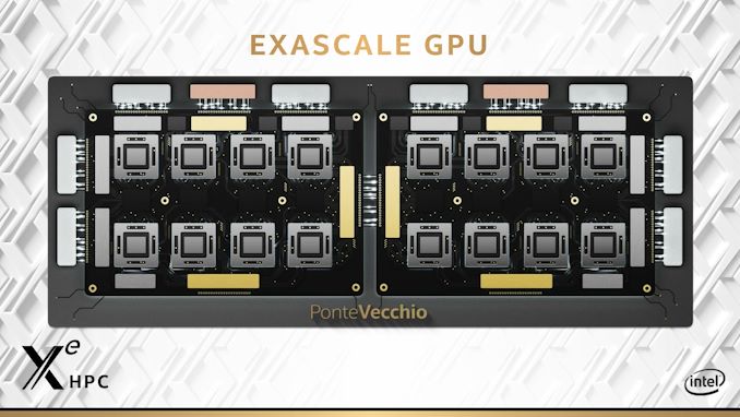
Better known by its codename of Ponte Vecchio, much to do has been made about Xe-HPC. The most complex of the Xe parts planned, it is also the cornerstone of the Intel-powered Aurora supercomputer. Xe-HPC is pulling out all of the stops for performance, and to get there Intel is employing every trick in the book, including their new-generation advanced packaging technologies.
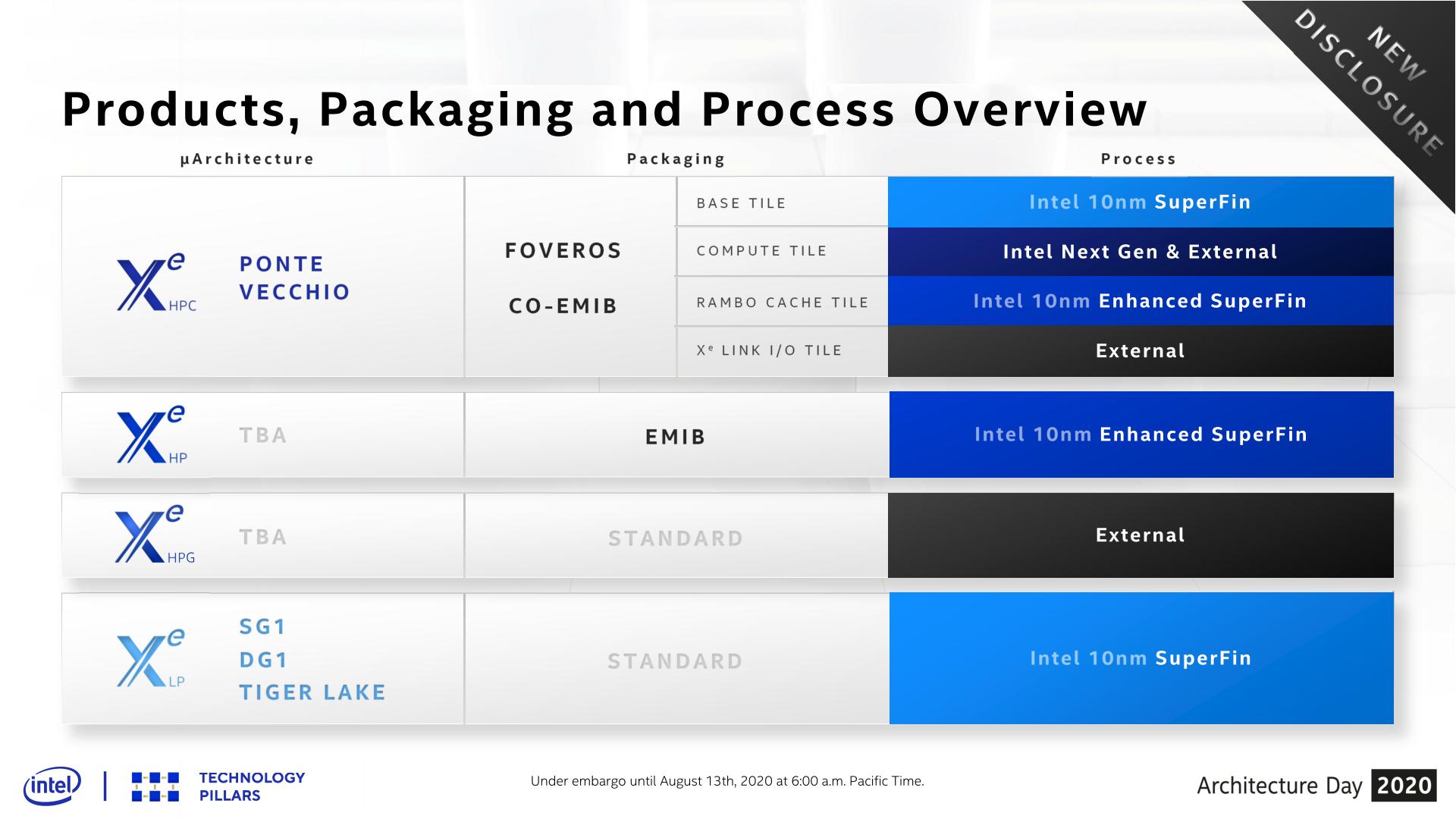
The big revelation here is that we finally have some more concrete insight into what manufacturing processes the various tiles will use. The base tile of the GPU will be on Intel’s new 10nm SuperFin process, and the Rambo Cache will be a generation newer still, using Intel’s future 10nm Enhanced SuperFin process. Meanwhile it’s now confirmed that the Xe Link I/O tile, which will be used as part of Intel’s fabric to link together multiple Xe-HPC GPUs, will be built by an external fab.
That leaves the matter of the compute tile, the most performance-critical of the GPU’s parts. With Intel’s 7nm process delayed by at least six months, the company has previously disclosed that they were going to take a “pragmatic” approach and potentially use third-party fabs. And as of their Architecture Day update, they still seem to be undecided about – or at least unwilling to disclose – just what they plan on doing. Instead, the compute die is labeled as “Intel Next Gen & External”.
It's an unusual disclosure, to say the least, as we'd otherwise expect the compute die to be made on a single process. But with no further commentary from Intel offered, make of that what you will. Perhaps they’re being straightforward, and they will actually use two very different process nodes for the compute die?


19 Comments
View All Comments
CityBlue - Thursday, August 13, 2020 - link
Is this Intel GPU glued together? Asking for a friend.dullard - Thursday, August 13, 2020 - link
Are you referring to AMD complaining that Intel's chips are glued together?Sahrin - Thursday, August 13, 2020 - link
I think he’s referring to Intel complaining that AMD’s chips are ‘glued together.’https://www.techpowerup.com/235092/intel-says-amd-...
dullard - Thursday, August 13, 2020 - link
Which was a response to AMD and AMD supporters saying it first back in 2006: https://www.computerworld.com/article/2818842/amd-...I'm just wondering if it is okay when AMD says it but not Intel.
dotjaz - Friday, August 14, 2020 - link
There's a big difference between talking through IO die on the same package and cores on the same die talking through off package NB via FSB. It's insane to pass information off package then back just to talk to each other.Spunjji - Friday, August 14, 2020 - link
"Which was a response"Not so much a response as a desperate callback to a diss laid out 11 years prior that referred to an entirely different set of technologies.
AMD's product that Intel accused of using "glue" was designed from the ground-up to be used with multiple dies on a single package communicating over a dedicated interconnect. Meanwhile, Intel's product that AMD had previously accused of using "glue" effectively took a dual-socket FSB-based-communication configuration and crammed it onto a single package, something they had done before with the Pentium D to no great acclaim.
So that's why some folks find it "okay" when AMD says it and "not" when Intel did - because there are material differences between the solutions being described this way. You *could* argue that there's similarity in the reasons *behind* the trash-talking, though. In both cases, it was a comment being made by a company who weren't able to compete on even terms with the product they were trying to demean.
dullard - Thursday, August 13, 2020 - link
Edit: that was even said back in 2005 from our own Anand: https://www.anandtech.com/show/1665/2PaulHoule - Thursday, August 13, 2020 - link
The disadvantage of "glued together" versus "smaller transistors" is that in the long term cost is proportional to die era, so it should be cheaper to deliver more transistors with by process shrink than by sticking together dies with a larger process.Advanced packaging is usually going to be expensive. Some cases might be simple (maybe you can come out ahead with 8 chiplets as opposed to 1 chip that is 8 times as large) and others offer high performance (HBM) which could translate to relative economy. But advanced packaging shines for low-volume expensive parts such as the brains for a Stinger missile.
Lord of the Bored - Friday, August 14, 2020 - link
Truly, our man Anand was a trendsetter.Null666666 - Thursday, August 13, 2020 - link
Glue is the firmware and software that negotiate the interconnects between the chip modules.