Qualcomm Launches Snapdragon Wear 3100 Platform for Smartwatches
by Anton Shilov on September 14, 2018 11:15 AM EST- Posted in
- SoCs
- Snapdragon
- Qualcomm
- Wearables
- Snapdragon Wear
Qualcomm this week introduced its new platform designed for smartwatches based on Google’s Wear OS. The long anticipated Snapdragon Wear 3100 packs four general-purpose processing cores as well a special co-processor for low-power operations designed to prolong battery life of upcoming wearables. Communication capabilities of the platform include GPS, Wi-Fi+Bluetooth, as well as 4G/LTE, which is in line with features supported by direct predecessor.
Qualcomm’s Snapdragon Wear 3100 (MSM8909w) is the company’s most powerful SoC for wearables that the company has released to date. Just like the Snapdragon Wear 2100 introduced in 2016, the new chip packs four ARM Cortex-A7 cores clocked at 1.2 GHz. Meanwhile, the latest SoC also integrates the company’s QCC1110 co-processor designed specifically for tasks that do not require serious compute horsepower, such as sensor processing in new modes to be supported by the upcoming version of Wear OS. The co-processor also has a deep learning engine for custom workloads like detection of keywords.
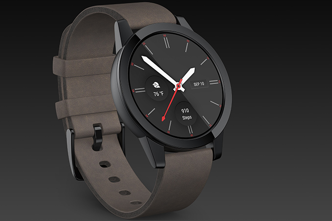
Besides general-purpose cores and the co-processor, the SoC integrates Qualcomm’s Adreno 304 GPU that supports resolutions up to 640x×480 at 60 Hz as well as a high-performance DSP. As for communication capabilities, the Snapdragon Wear 3100 platform can support Qualcomm’s WCN3620 Wi-Fi/Bluetooth controller, Qualcomm’s Snapdragon X5 4G/LTE modem, and GPS capabilities. Meanwhile, the company will offer three versions of the SW3100 targeting smartwatches with different comm features.
Qualcomm says that it works closely with developers of Google’s Wear OS, so all the capabilities of the new Snapdragon Wear 3100 platform will be used by software eventually. In particular, the SW3100 will support three modes that will be a part of next-gen watches running the Wear OS, including the Enhanced Ambient Mode, Dedicated Sports Experiences, and Traditional Watch Mode. In all three cases the SW3100 will offload display and sensor processing from the Cortex-A7 and Adreno cores to the ultra-low-power co-processor, but will still be able to perform typical tasks for each mode (e.g., GPS and heart rate sensing for the sports mode).
| Qualcomm Snapdragon Wear SoCs | ||||
| Snapdragon Wear 1200 | Snapdragon Wear 1100 | Snapdragon Wear 2100 | Snapdragon Wear 3100 | |
| SoC | Cortex-A7 @ 1.3GHz Fixed-function GPU |
Cortex-A7 @ 1.2GHz Fixed-function GPU |
4x Cortex-A7 @ 1.2GHz Adreno 304 |
4x Cortex-A7 @ 1.2GHz QCC1110 co-processor Adreno 304 |
| Process Node | 28nm LP | 28nm LP | 28nm LP | ? |
| RAM | LPDDR2 | LPDDR2 | LPDDR3-800 MT/s | LPDDR3 (?) |
| Display | Simple 2D UI | Simple 2D UI | Up to 640x480 @ 60fps | |
| Modem | Qualcomm (Integrated) 2G (E-GPRS) / LTE (Cat M1 & Cat NB1) |
Qualcomm (Integrated) 2G / 3G / LTE (Category 1 10/5 Mbps) |
Qualcomm X5 (Integrated) 2G / 3G / LTE (Category 4 150/50 Mbps) Connected version only |
|
| Connectivity | 802.11b/g/n/ac, BT 4.2 LE, GPS/GLONASS/Galileo/BeiDou | 802.11b/g/n/ac, BT 4.1 LE, GPS/GLONASS/Galileo/BeiDou (Wi-Fi and BT optional) |
802.11b/g/n (2.4GHz), BT 4.1 LE, NFC, GPS/GLONASS/Galileo/BeiDou, USB 2.0 Connected and Tethered versions |
|
Qualcomm claims that the QCCC1110 co-processor, the PMW3100 power management sub-system, and other enhancements of the Snapdragon Wear 3100 will help to reduce the SoC's power consumption rather significantly. The net benefit from this, according to Qualcomm, is that device makers will be able to prolong the battery life of their devices by 4 to 12 hours when compared to the previous-generation Snapdragon Wear 2100 platform.
Qualcomm says that mass production of the Snapdragon Wear 3100 had already started, as have shipments to customers. The first companies to adopt the new SoC are Fossil Group, Louis Vuitton, and Montblanc.
As is usually the case for the chip vendor, Qualcomm is not disclosing when their customers intend to release their SW3100-powered watches to consumers. However what we're hearing from other sources is that the first watches should hit store shelves next month, in which case we're looking at a relatively quick turnaround time here.
Related Reading:
- Qualcomm Announces Snapdragon 2500 Wearable Platform For Kids Watches
- Qualcomm Announces Snapdragon Wear 1200 SoC: LTE Categories M1 & NB1 for Wearables & Smart Trackers
- ASUS ZenWatch 3 Announced: Round Display, Snapdragon Wear 2100, Long Battery Life
- Qualcomm Announces Snapdragon Wear 1100 SoC For Wearables
- Qualcomm Announces Snapdragon Wear 2100 IoT SoC
Source: Qualcomm


43 Comments
View All Comments
tipoo - Friday, September 14, 2018 - link
Still 28nm, still Cortex A7...Seems like the absolute minimum response to complaints that the 2100 was holding WearOS back. Meanwhile S4 has gone 64 bit, die shots will tell the manufacturing node.Drumsticks - Friday, September 14, 2018 - link
Is it still 28nm? The table has a question mark.If it is, it is somewhat surprising, but not crazy. I can't imagine they expect to make tons of money off of this, so the cheapest process possible is probably what they're going for.
hertzsae - Friday, September 14, 2018 - link
It's been confirmed elsewhere that it's 28nm. Qualcomm has also stated that the main CPU is essentially unchanged from the 2100. It's clear they did not allocate a lot of budget, otherwise we would see a A35 based chip instead of the same A7 chip from a few years ago.tuxRoller - Friday, September 14, 2018 - link
The a32 is even more efficient than the a7(it's also aarch32 so you get massive speedups for certain instructions).As others sites have noted, the most interesting aspect to this soc is the new low power core.
Gadgety - Saturday, September 15, 2018 - link
Yes, that table needs to be updated.V900 - Friday, September 14, 2018 - link
Yes, clearly smart watches that are still held back by battery capacity need more powerful CPUs chucked at them! 🙄The Apple Watch using a 64 bit CPU does absolutely zero in terms of performance or battery usage, it’s just an Apple thing, since they want all of their codebase to switch to 64 bit.
tipoo - Friday, September 14, 2018 - link
Ugh, what year is it.More capable CPUs can also reduce power usage if they complete a task with similar peak power, in less time, and get to sleep faster.
And shrinking to 14, leave alone 7nm, would increase the processors efficiency over the old 28nm node. Like, where have you been, that's not news.
V900 - Friday, September 14, 2018 - link
It’s the year where I’m right and you’re wrong.Unless you think Qualcomm is exclusively staffed by idiots, there’s a good chance that they know what they’re doing, and prob. have a better grasp of designing an SOC than your average Anandtech poster.
The A7 is more energy efficient than newer ARM cores, and it’s more than fast enough for a Watch. (Heck, they have tablet SOCs running with Quad or Octa core A7 CPUs on them, so saying things somehow not powerful enough for a Watch is ridiculous.)
You could get an SOC using even less power on a newer node, but who’s going to pay for it.
Smartwatches aren’t exactly in hot demand, and the ones that do sell are the lower priced ones.
And good luck making a 200$ device, with a SOC that’s 2-3 times as expensive because it’s on a 14nm node or even worse: A 7nm node.
Gadgety - Saturday, September 15, 2018 - link
It's the who's paying and a volume issue, for Qualcomm, absolutely. Cost, cost, cost. The solution they have come up with is pretty smart considering that they stay on the 28nm. If I get 15 hours of simultaneous HRM and GPS which is their claim, it'll be more than sufficient, for my needs at least.WPX00 - Saturday, September 15, 2018 - link
Because A7 is no longer powerful enough. My ZenWatch 2 lags like s*** on its Snapdragon 400 processor, and theres nothing that's meaningfully changed on these processors that suggests it will be different.