Intel to Equip Fab 42 for 7 nm
by Anton Shilov on February 9, 2017 4:45 PM EST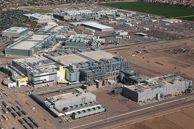
Intel this week announced plans to bring its Fab 42 online to produce semiconductors using a 7 nm fabrication process. It will take three to four years, and the move will cost Intel several billions of dollars but will create approximately 3,000 of high-tech jobs in Chandler, Arizona. Unfortunately, Intel did not share details about its 7 nm manufacturing technology at this time.
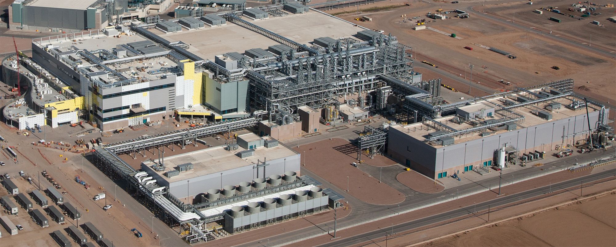
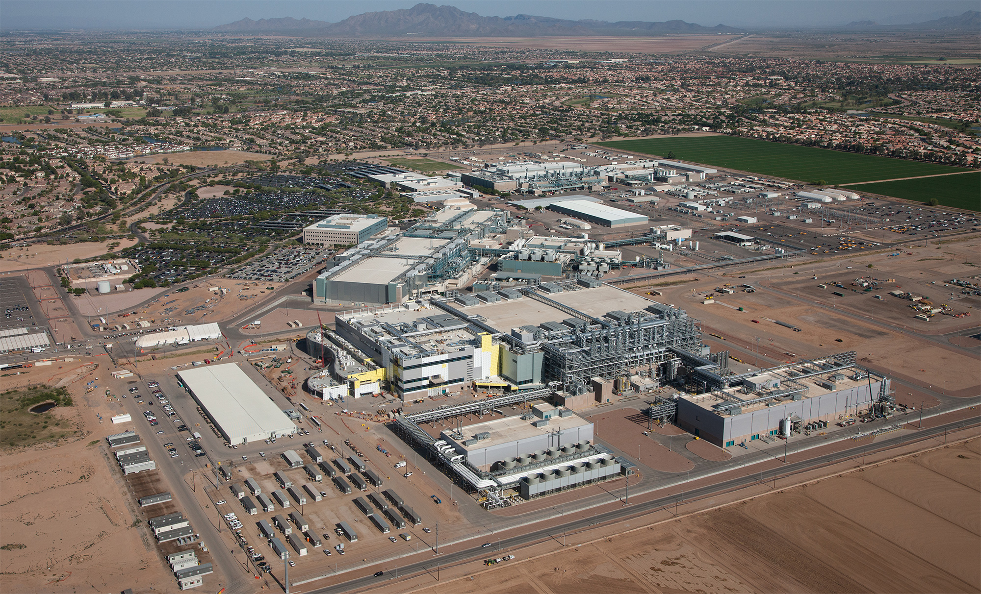
Intel began construction of its Fab 42 back in 2011 with the aim to build the most advanced, high-volume chip production facility in the world. The building was completed in 2013, but instead of moving in equipment to produce chips using 14 nm fabrication process, Intel decided to postpone its completion in early 2014. The site is equipped with heating, air conditioning, and other essential things, but no actual semiconductor manufacturing equipment has been installed. Intel still has no immediate public plans to use the Fab 42 for the production of chips using its 10 nm process technology in the short-term future but has indicated it intends to use it for its 7 nm ICs several years down the road.
Intel intends to spend as much as $7 billion to equip Fab 42, but at the moment the company does not share what kind of tools it plans to install. As a result we have no new information about Intel's 7 nm technology. Intel has implied that it could start using extreme ultraviolet (EUV) lithography at 7 nm, but has never committed to the plan. Earlier this year the company said it would invest in a 7 nm pilot line in one of its development sites, but did not elaborate beyond that. One of the things that the CEO of Intel disclosed about the 7 nm in general in his email to employees this week is that it requires “an increasing amount of factory space per wafer.” This possibly means that Intel will insert EUV equipment into the process technology for cirical layers and will continue to use a lot of multipatterning, which increases the diversity requirements for the production tools.
Intel believes that when completed, Fab 42 will be the most advanced semiconductor wafer fab in the world that will create 3,000 direct high-tech jobs and 10,000 direct and indirect jobs in total. It should be noted that the semiconductor company will not start to move in equipment into the Fab 42 before it figures out all the peculiarities of the 7 nm manufacturing technology. Once it finalizes the pilot line and is satisfied with the equipment performance, it starts to replicate the line at different sites.
Intel said that it will use its 7 nm fabrication process to produce various processors for PCs, data centers and other devices that will be used for AI, automated driving, medical research/treatment as well as other applications. So, as usually, the manufacturing technology will be positioned to make the whole stack of Intel’s products several years from now.
Related Reading:
Source: Intel


24 Comments
View All Comments
Morawka - Thursday, February 9, 2017 - link
I wonder if they will use silicon germanium and EUV on their 7nm. i would suspect so since they reserved this site for 7nm. If they were using traditional techniques, they would have probably upgraded existing facilities instead of starting fresh with fab42.Stochastic - Thursday, February 9, 2017 - link
The generational gains, both in terms of IPC and load power efficiency, have been minimal since 2012 for Intel. Is there any sign of this changing in the next five years? Or are we just too deep into the diminishing returns curve for Intel's architecture?ddriver - Thursday, February 9, 2017 - link
They mostly care about how small they can make the chip to maximize profit. But it is not entirely their fault, process will soon hit a brick wall and come to a stand still. And all the "graphene and nanotubes will revolutionize chips" stuff is nowhere near commercially feasible, nor is the outlook on new process technology optimistic.Stochastic - Friday, February 10, 2017 - link
I thought we were past the point where node shrinks decrease per CPU production costs?willis936 - Friday, February 10, 2017 - link
I can't think of a reason that would ever be the case. If it takes you $10,000 to make a wafer wouldn't you rather get 120 chips out of it rather than 100? There's always an economic benefit to making it smaller. When it becomes too costly to make it smaller then they'll stop going smaller. I don't think performance drives the technology as much as money.3DoubleD - Friday, February 10, 2017 - link
I think the cost per chip hasn't been falling significantly or at all because the die sizes haven't been decreasing. In the recent i3 K-series review on Anandtech, they showed a plot that demonstrated this perfectly - die sizes are stagnant. YES, you get more transistors and performance with each generation and the cost/transistor or cost/performance drops, but this is because more transistors are crammed into the same area or are utilized more efficiently.With die sizes stagnant, the cost per wafer is stagnant or increasing unless they can increase the wafer size in a profitable way. This comes with its own issues though.
Factoring in that the technologies required to produce "7 nm" node wafers are temperamental (EUV) or has reduced throughput (multipatterning), price per wafer (and per die at fixed die sizes) is bound to increase (or have already started to increase).
ddriver - Friday, February 10, 2017 - link
It is curious that die sizes remain stagnant while at the same time that is also true for performance. It begs the question, if the transistor count increase is nowhere near the modest performance gains we see, what exactly is intel investing those transistors into?Skynet?
From the looks of it, we might actually begin to see regressions in terms of efficinecy in upcoming process nodes. All in the name of shrinking things down and cramming more transistors in there. But why? Maybe intel is just bent on keeping moore's nonsensical law alive, which in their interest is about transistor count only, not about performance or any meaningful metric, are they merely cramming more transistors for the sake of keeping the pipe dream of infinite scaling alive, or are they doing something pointless, or even sinister with those transistors?
phoenix_rizzen - Saturday, February 11, 2017 - link
Most of the die goes to the GPU these days. The actual CPU cores are tiny in comparison.HStewart - Thursday, December 6, 2018 - link
First of all this is not just Intel on investing where transistors are going. As for Skynet and AI push, I believe we are seeing that more on GPU side - especially with NVidia and even ARM based stuff.As for keeping size down, it probably more aim at mobile - but if you think about - smaller the distance less electrons have to travel.
As for infinite scaling, Xeon scalable can scale up to 500+ cpus - and that independent of cpu cores. I am not sure this is concern, but I would think that huge dies would be fragile.
One thing I like is idea of EMiB, it is nice idea that CPU and even GPU can be smaller size chip while IO and other components can be larger size chip on same package. It just seem not that logically to put everything on more dense chip unless you have the ability. Also mix and match of components is a good things - especially when discussing mobile world.
The world has change, mobile world is pretty much driving the technology and desktop world is just coming a long for the ride.
Jaybus - Tuesday, February 14, 2017 - link
Not really. The process equipment also gets more complicated and more expensive. The Van der Waals radius of Si is 210 pm. 7 nm is about 17 atoms wide. It is just incredibly small. The hard limit is of course one atom, but the reliability of current flow erodes well before that. More than likely, not too many die shrinks remain possible for Si-based wafers. My guess is a move to photonic devices, rather than electronic. In particular, photonic chip-to-chip interfaces could play a large role. For example, a photonic memory bus could be many times faster than on-chip RAM, allowing the elimination of on-chip L2 and L3 cache. That alone would reclaim a huge amount of real estate that could then be used to increase logic gate count without a die shrink.