A Few Notes on Intel’s Knights Landing and MCDRAM Modes from SC15
by Ian Cutress on November 16, 2015 5:41 PM EST- Posted in
- CPUs
- Intel
- HPC
- Enterprise
- Trade Shows
- Xeon Phi
- Omni-Path
- Knights Landing
- SC15
- MCDRAM
When learning about new hardware, there are always different angles to look at it. For the most part, manufacturers talking to the media will focus on the hardware aspects of the new shiny thing, about what it can do at a high level then go into a low level silicon architecture detail (sometimes). Anything on the software side comes through talks about how to write for the new shiny thing – this is why Intel has conferences such as IDF (Intel Developer Forum) to help explain how to use it. Interestingly there can always be information about the true operating nature of the device in a software talk, as opposed to a hardware talk.
As such, I attended a tutorial session here at SuperComputing15 on the MCDRAM (Multi-Channel DRAM) used in Intel’s 2nd generation Xeon Phi, code named Knights Landing (KNL). Specifically the talk focused on the analysis methods and tools, and it went into greater depth as to how the implementation works.
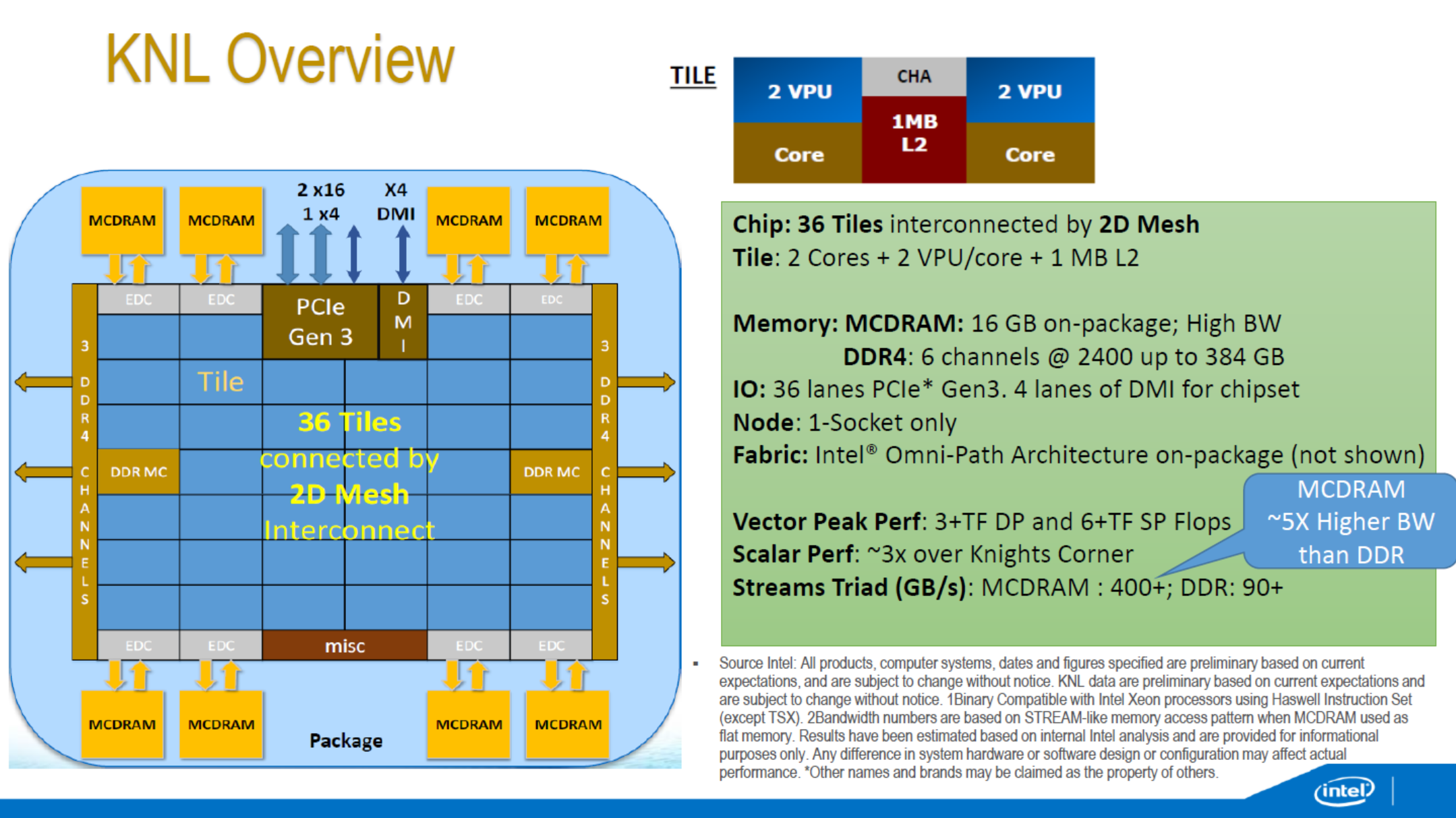
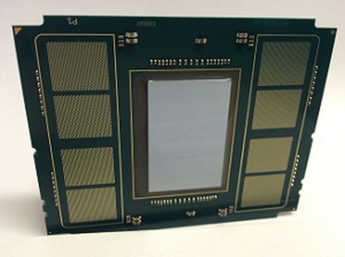
Some of the KNL overview we have seen before – the 72 Silvermont-based cores running at ~1.3 GHz are split into tiles with two cores per tile, two VPUs (Vector Processing Units, AVX-512) per core and each tile shares 1MB of L2 cache for a total of 36MB of L2 across the design. Rather than the ring topology we see in the standard processor designs from Intel, they are arranged in a mesh topology using an interconnected fabric (which seems to be sets of rings anyway). Despite the 6x7 nature of the image above, shots of the package have had some question that the layout is more akin to a 4x9, although this is unconfirmed.
The big paradigm shifts are everywhere. KNL can be used as the main processor in a computer, running an OS on top of all the cores, or as a co-processor similar to former Xeon Phi silicon – but as noted above in the slide there is no version of QPI for 2P/4P systems. There are a total of 36 PCI 3.0 lanes though, for PCIe co-processors, as well as onboard Omni-Path control for network interconnects. The cores are 14nm versions of Silvermont, rather than 22nm P54C, with claims that the out-of-order performance is vastly improved. The die has a total of 10 memory controllers – two for DDR4 controllers (supporting three channels each), and then eight for MCDRAM.
Each of these high-bandwidth controllers link out to a the on-package MCDRAM (we believe stacked 20nm Micron Planar DRAM) through an on-package interposer, offering 400+ GB/s of bandwidth when all the memory is used in parallel. This sounds similar to AMD’s Fiji platform, which offers 4GB of memory over four HBM (high bandwidth memory) packages, but Intel is prepared to offer 16GB of MCDRAM ‘at launch’. The fact that Intel says at launch could be suggested that there are plans to move into higher capacities in the future.
As the diagram stands, the MCDRAM and the regular DDR4 (up to six channels of 386GB of DDR4-2400) are wholly separate, indicating a bi-memory model. This stands at the heart at which developers will have to contend with, should they wish to extract performance from the part.

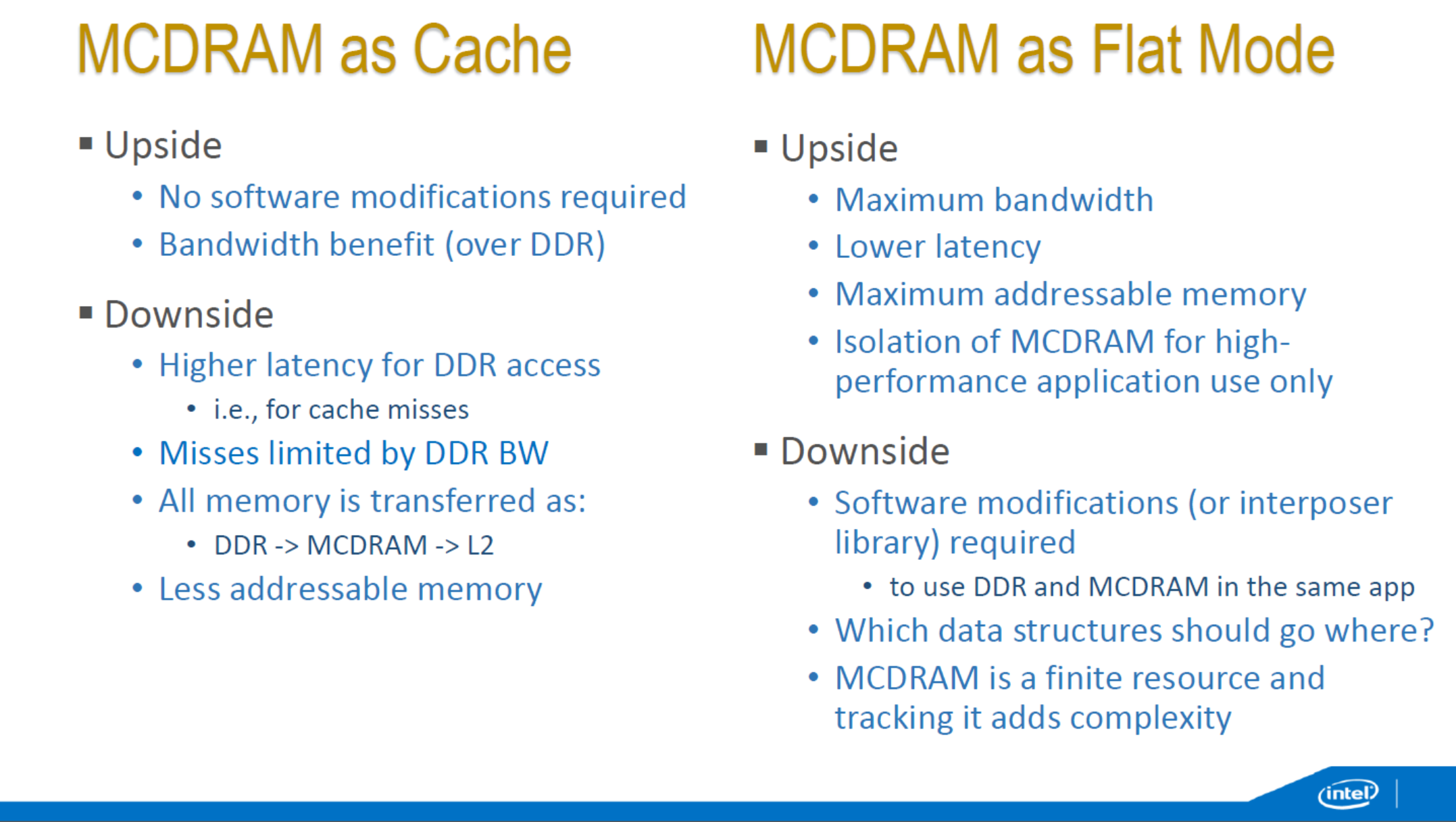
The KNL memory can work in three modes, which are determined by the BIOS at POST time and thus require a reboot to switch between them.
The first mode is a cache mode, where nothing is needed to be changed in the code. The OS will organize the data to use the MCDRAM first similar to an L3 cache, then the DDR4 as another level of memory. Intel was coy onto the nature of the cache (victim cache, writeback, cache coherency), but as it is used by default it might offer some performance benefit up to 16GB data sizes. The downside here is when the MCDRAM experiences a cache miss – because of the memory controllers the cache miss has to travel back into the die and then go search out into DDR for the relevant memory. This means that an MCDRAM cache miss is more expensive than a simple read out to DDR.
The second mode is ‘Flat Mode’, allowing the MCDRAM to have a physical addressable space which allows the programmer to migrate data structures in and out of the MCDRAM. This can be useful to keep large structures in DDR4 and smaller structures in MCDRAM. We were told that this mode can also be simulated by developers who do not have hardware in hand yet in a dual CPU Xeon system if each CPU is classified as a NUMA node, and Node 0 is pure CPU and Node 1 is for memory only. The downside of the flat mode means that the developer has to maintain and keep track of what data goes where, increasing software design and maintenance costs.
The final mode is a hybrid mode, giving a mix of the two.
In flat mode, there are separate ways to access the high performance memory – either as a pure NUMA node (only applicable if the whole program can fit in MCDRAM), using direct OS system calls (not recommended) or through the Memkind libraries which implements a series of library calls. There is also an interposer library over Memkind available called AutoHBW which simplifies some of the commands at the expense of fine control. Under Memkind/AutoHBW, data structures aimed at MCDRAM have their own commands in order to be generated in MCDRAM.
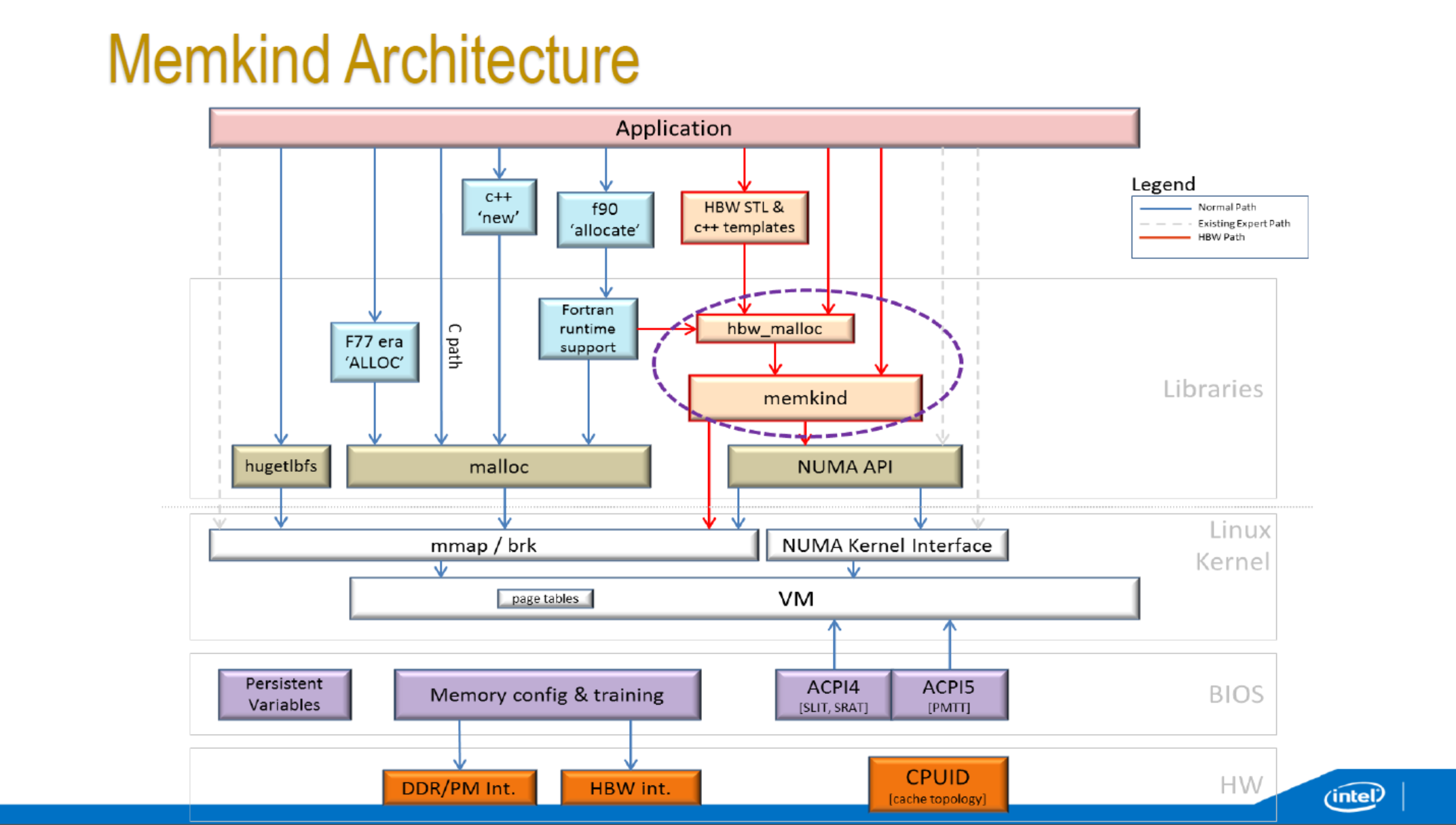
Intel’s VTune utilities will be enabled with KNL from VTune Amplifier XE2016.
There was some talk regarding Intel’s upcoming 3D XPoint which offers another layer of memory but this time in a non-volatile format. We were told to expect 3D XPoint to become a part of future Xeon Phi designs, along with multi-level memory management (potentially three: MCDRAM, DDR, XPoint), although the exact nature of how many levels of memory, or what types and how to use them, is still undecided. What we do know about the future is that the 3rd generation of Xeon Phi will be built on 10nm and named Knights Hill, featuring 2nd generation Omni-Path host fabric.


10 Comments
View All Comments
Vlad_Da_Great - Monday, November 16, 2015 - link
It seems INTC is attacking hard the HPC and Co-Processor market. NVDA is in trouble. "The downside of the flat mode means that the developer has to maintain and keep track of what data goes where, increasing software design and maintenance costs." Duh, that is why the libraries are developed and developer doesnt need to know anything, just pull the strings and drop the require or include.ABR - Tuesday, November 17, 2015 - link
I wouldn't put it so much as Nvidia is "in trouble" as Nvidia has some competition. It's going to get more interesting though. Both are coming into this relatively smaller market from different directions, each adapting their hardware from its original purposes. Intel from above, Nvidia from below, each working to build the software support around it. AMD continues to work its angle with heterogenous systems. Despite x86 it's actually Nvidia with the early lead on the software side, but they'll have to work to preserve it. Interesting times.BurntMyBacon - Wednesday, November 18, 2015 - link
@ABR: "Despite x86 it's actually Nvidia with the early lead on the software side, but they'll have to work to preserve it."I generally agree with your post accept I'm not so sure about this. There are many supercomputers out there with nothing but Intel Xeons or AMD Opterons. They've been out much longer than the Tesla processors. I'd guess that Intel is further along on the software side. There is some work to be done to adapt code from many complex cores to many simple cores, but they are all OoO x86 cores with largely the same features. I would think that these adaptations would be easier than adapting for CUDA and its similar changes and caveats for successive generations of GPUs. Their is no denying that nVidia has done a good job building up their software, though. Limiting to just CUDA/OpenCL, I have no doubt that their ecosystem is more rubust.
I think that AMDs heterogeneous vision is ideally the best, but AMD is having a hard time converting that vision into a desirable product. Given that HSA isn't closed (ARM vendors are planning to use it) nVidia and Intel could have already capitalized on AMD's vision if they weren't so preoccupied with making sure that their technologies remain proprietary. I guess standardization and interoperability don't generate sales in today's market.
ABR - Wednesday, November 18, 2015 - link
@BurntMyBacon : I also pretty much agree with the points you make. The question though is where exactly is the sweet spot of that market they are defining and trying to move into? It actually isn't traditional supercomputing, even though Nvidia is making efforts there. Right now it's smaller scale stuff growing out of people wanting to do more with their workstations now that CPU speeds have stagnated. The scientists, the creatives, crypto guys, a groundswell of people picking up GPUs to get those order of magnitude improvements that used to come biannually in PCs. This is where CUDA has been strong. Few have the budget to build and maintain a "Beowulf" cluster let alone something bigger, but slapping a few Tesla cards into a box has been a lower barrier to entry. Low enough to justify writing software and letting an ecosystem grow. And the data center / cloud GPU compute trends are growing out of this same category of users. The cloud is most alluring to those wanting to stretch a thin budget far. This is the growth area being fought for.patrickjp93 - Saturday, November 21, 2015 - link
Intel's tech isn't proprietary. OpenMP has been around since 2000 and went open standard in the early 2000s. It's the bread and butter of intel-based supercomputers today. It's also vastly superior to HSA implementations in programmability.patrickjp93 - Saturday, November 21, 2015 - link
I'm sorry but Intel definitely has the software ecosystem advantage. Intel-based supercomputers have been built around OpenMP for years. Do you know how easy it is to adapt code to send it to the Xeon Phi? You literally wrap it with 1 line of header and two braces.#pragma offload target(mic) map(some_vector[i:N]) in(result_vector){
//the same openmp/C++ parallel code you had in here before
}
vFunct - Tuesday, November 17, 2015 - link
This + 32GB of MCDRAM + several TB of X-Point would make a killer cloud server.bds71 - Tuesday, November 17, 2015 - link
replace 24 of those cores with GPU cores; and, (when stacked RAM becomes available) stack XPoint on top of MCDRAM. you now have CPU, GPU, RAM, and Storage on a single chip = complete PC!!questionlp - Tuesday, November 17, 2015 - link
"As the diagram stands, the MCDRAM and the regular DDR4 (up to six channels of 386GB of DDR4-2400) are wholly separate, indicating a bi-memory model."That should be 384GB, not 386GB
iAPX - Friday, November 20, 2015 - link
16GB is good for small to medium-sized vectorized problems, 384GB is an huge step forward for highly parallelized architectures, still the low bandwidth of DDR4 and the implicitly sequential nature of x86 code processing on Knight Landing (compared to GPU that will launch MANY pseudo-threads to try to hide memory latencies) will creates bubbles in the pipelines (huge bubbles!) if there are cache miss or direct DDR4 accesses.The DDR4 itself with it's 6 controllers is a low-bandwidth <100GB/s memory, compared to actuel graphic cards, in fact it's playing against 99$ and undr graphic cards!
Question is, will 16GB of MCDRAM be enough, and it could be as nearly all GPGPU sub-systems doesn't have as much memory, or will programmers use the huge available DDR4 memory?
I think the answer is in th hands of the developers.