Intel’s Three Versions of Socket 2011, Not Compatible
by Ian Cutress on February 20, 2014 9:45 AM EST- Posted in
- CPUs
- Intel
- Xeon
- LGA2011
- Ivy Bridge EX
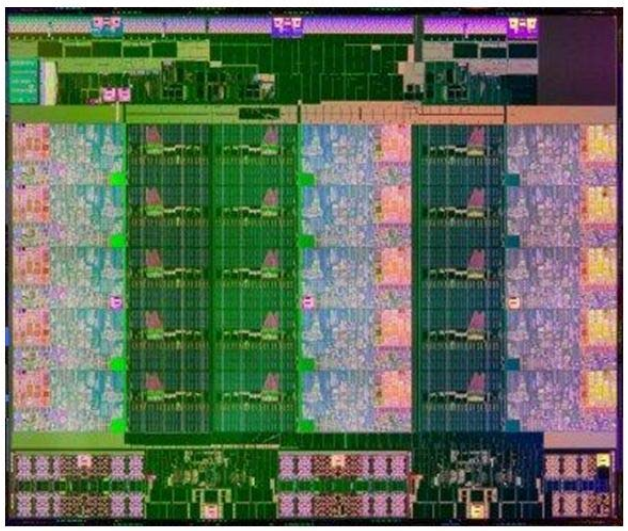
With our recent discussion regarding Intel’s launch of the 15-core Xeon E7 v2 ‘IvyTown’ processors, thoughts for a lot of high end consumers focused on the underlying hardware for these 4P and 8P systems that would be entering the market. Previously with high end systems there has been a disjunct between the sockets used for the mainstream 1P and 2P processors (-E and -EP) compared to the higher end 4P/8P models (-EX). For example:
With Nehalem/Westmere, the single socket Bloomfield Xeons were LGA 1366.
With Nehalem-EP/Westmere-EP, the dual socket Gainstown Xeons were also LGA 1366.
With Nehalem-EX/Westmere-EX, the quad/octo socket Beckton Xeons were LGA 1567.
With Sandy Bridge-E/Ivy Bridge-E, the single socket Xeons are LGA 2011.
With Sandy Bridge-EN/Ivy Bridge-EN, the single/dual socket Xeons are LGA1356
With Sandy Bridge-EP/Ivy Bridge-EP, the dual socket Xeons are LGA 2011.
With Ivy Bridge-EX, the quad/octo socket Xeons are also LGA 2011, but different.
Reported images of Haswell-EP Xeons also point to LGA 2011, but different again.
Back at ISSCC, when we reported about the talk around the new IvyTown based processors, we lifted the following line from the official documentation:
- “The processor supports two 2011-land, 40-mil pitch organic flip-chip LGA package options”
This produced speculation to whether the processor package for EX would be the same as EP, despite a reconfigured memory controller, additional QPI links and a different pin layout. Given at the time we were under NDA we could not mention they were different, but some investigative work from Patrick at ServeTheHome answers a lot of questions.
Simply put, Ivy Bridge-EP, Ivy Bridge-EX and Haswell-EP all have LGA2011 designations (officially FCLGA2011, for flip-chips), but have different physical mountings in the socket:
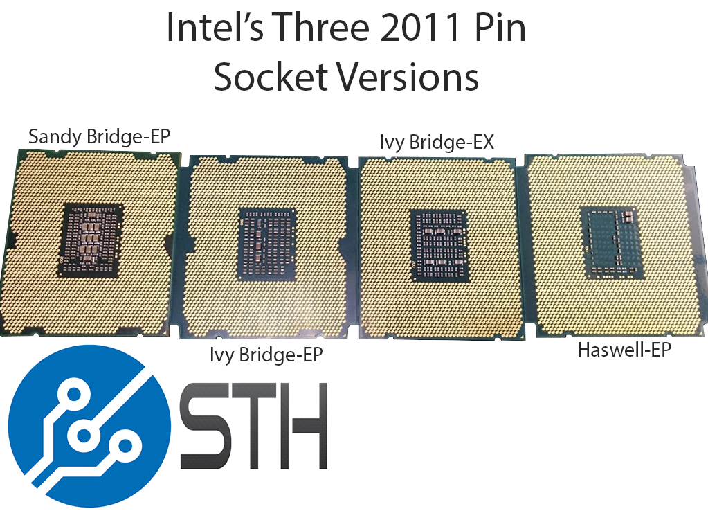
Despite the contact patches/‘wings’ on Ivy Bridge-EP, it will fit in the Sandy Bridge-EP socket – the issue is more the pins on Ivy Bridge-EX and Haswell-EP, where on the left and right it is more ‘filled in’, as well as at the corners. The notches for the processors (the indents on the top and bottom) are also different, moving to Ivy Bridge-EX.
The Ivy Bridge-EX and Haswell-EP processors look very similar from these images, despite the extra wings on the Haswell-EP. The key here is the bottom right of the two processors, and count the number of pins between the notch and the edge – Ivy Bridge-EX has four, Haswell-EP has six.
All in all, this may not much of anything – users spending thousands on processors should be making sure that the motherboards they buy have the processor they want listed in the QVL (Qualified Vendor’s List). My concern might be users thinking they can drop a Haswell-EP Xeon into an Ivy Bridge-E, and then trying to force it when it might not fit. Back in previous eras (socket 775 comes to mind) this was an even bigger issue – the processors might fit, but the processors that a motherboard could take was determined by the chipset used by the motherboard manufacturer and the QVL. At least this way the CPUs will not physically fit, but it is something that confuses the situation – it might be worth doing some clever renaming (LGA2011-EX, LGA2011-H), at least from an editorial point of view for the future.
Source: ServeTheHome


47 Comments
View All Comments
Lerianis - Thursday, February 20, 2014 - link
3 different processor port designs? Intel, what the hell were you thinking here? You come out with ONE port design or at the most two that are mutually exclusive, one for servers and one for regular desktops/laptops.I am seeing a lot of people with blown processors in the future due to this.
GL1zdA - Thursday, February 20, 2014 - link
And how do you expect one socket for processors with different features? The EX uses 4 QPI links, the EP 2 QPI links, the Haswell-EP will use DDR4 - how many contacts should your "one socket to rull them all" have? Ten thousand?fokka - Thursday, February 20, 2014 - link
you are right, but simply naming all lga 2011 still is a stupid idea.dylan522p - Thursday, February 20, 2014 - link
Why? Anyone who cares knows.repoman27 - Thursday, February 20, 2014 - link
And if the we're talking about a 2011-land Land Grid Array package, then LGA2011 is how we'd refer to it. There are plenty of semiconductor manufacturers that produce similar packages that are not pin compatible or even related, e.g. QFN64 or TSOP28.Intel refers to the sockets as "Socket R", "Socket R1" and "Socket R3".
repoman27 - Thursday, February 20, 2014 - link
And the packages and corresponding sockets (or ILMs in Intel parlance) are keyed differently, so you'd likely break something before you could cause electrical damage to the processor by inserting it into an inappropriate system.HisDivineOrder - Thursday, February 20, 2014 - link
Someone who cares won't know. It's inevitable. There'll be that one guy complaining on a forum somewhere about how he was completely surprised by this.Inevitably, his name will be Larry. Or Bob.
LordOfTheBoired - Friday, February 21, 2014 - link
Why name them at all, then? If the name is useless, and they've created a situation where IT IS, just don't give the socket a name.I'd rather see them say nothing at all about the socket than than give a slew of different and largely unrelated connections a shared name. This is actually a WORSE situation than if the motherboard and processor specs said nothing about compatibility, because now someone who is unsure can check a bullet list, see that he has an LGA2011 processor and an LGA2011 motherboard, and expect them to work. With NO ready compatibility information, he will be FORCED to either do the necessary research or buy AMD out of sheer frustration. And this is dumb enough that "AMD has an agent inside Intel sabotaging the company" is the MOST rational explanation, which says a LOT about how insane this mess is.
Kevin G - Thursday, February 20, 2014 - link
There can be multi-purpose pins that are configured upon boot. For example, pins for 8 lanes of PCI-e could be configured to be an extra QPI link (note that Ivy Bridge-EX only has 32 PCI-e lanes instead of the 40 on EP version). Ditto for the memory bus pins: reuse them for DDR3, DDR4 and the serial memory buffers. The pin count would increase but not drastically so.This is especially more pronounced with socket 1156/1155/1150. The main difference between them was display out and clock generation. Intel could have easily a few extra pins for display IO growth, ignored the external clock input on later CPU's and kept the consumer line on the same socket for the past 5 years.
ZeDestructor - Thursday, February 20, 2014 - link
Utterly pointless though, since you still have to change motherboards because you need a new chipset.On the other hand, within LGA1155, you can use both Sandy Bridge and Ivy Bridge with no issues (bessides possible UEFI updates, and being limited to PCIe 2.0 on x6x compared to PCIe 3.0 on x7x boards)
I for one do not lament moving away from the LGA775 years of choosing which chipset and which motherboard implementation of said chipset supports the CPU I have.
So far Intel has kept the sockets inline with chipset and power requirements since LGA1366. It is true that I can't replace my motherboard with a newer board if my current one dies, but tbh, it's made my life easier: Gen X with chipset series Y will work across the entire generation, and by the time a motherboard dies, I want a new CPU as well.....