Intel's 50Gbps Silicon Photonics Link: The Future of Interfaces
by Brian Klug on July 30, 2010 6:49 AM EST- Posted in
- Trade Shows
- Intel
- Photonics
- Laser
On Tuesday, Intel demonstrated the world’s first practical data connection using silicon photonics - a 50 gigabit per second optical data connection built around an electrically pumped hybrid silicon laser. They achieved the 50 gigabit/s data rate by multiplexing 4 12.5 gigabit/s wavelengths into one fiber - wavelength division multiplexing. Intel dubbed its demo the “50G Silicon Photonics Link.”
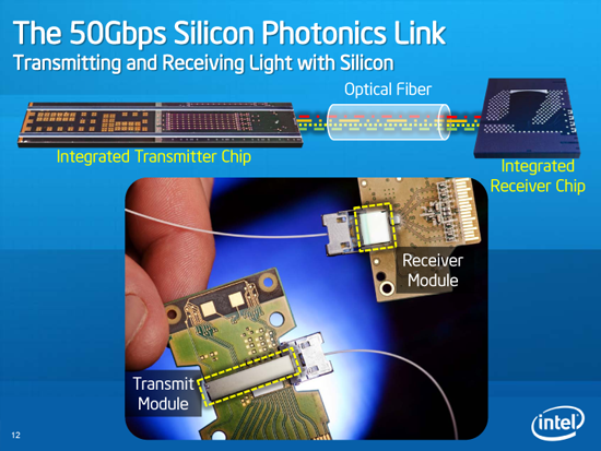
Fiber optic data transmission isn’t anything new - it’s the core of what makes the internet as we know it today possible. What makes Intel’s demonstration unique is that they’ve fabricated the laser primarily out of a low-cost, mass-produceable, highly understood material - silicon.
For years, chip designers and optical scientists alike have dreamt about the possibilities of merging traditional microelectronics and photonics. Superficially, one would expect it to be easy - after all, both fundamentally deal with electromagnetic waves, just at different frequencies (MHz and GHz for microelectronics, THz for optics).
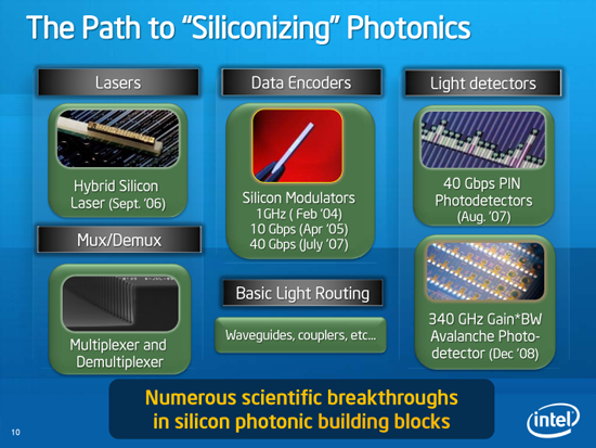
On one side, microelectronics deals with integrated circuits and components such as transistors, copper wires, and the massively understood and employed CMOS manufacturing process. It’s the backbone of microprocessors, and at the core of conventional computing today. Conversely, photonics employs - true to its name - photons, the basic unit of light. Silicon photonics is the use of optical systems that use silicon as the primary optical medium, instead of other more expensive optical materials. Eventually, photonics has the potential to supplant microelectronics with optical analogues of traditional electrical components - but that’s decades away.
Until recently, successfully integrating the two was a complex balance of manufacturing and leveraging photonics only when it was feasible. Material constraints have made photonics effective primarily as a long haul means of getting data from point to point. To a larger extent, this has made sense because copper traces on motherboards have been fast enough, but we’re getting closer and closer to the limit.


42 Comments
View All Comments
dasHHa - Friday, July 30, 2010 - link
Moore's law still going on!Muscles - Friday, July 30, 2010 - link
A lot to look forward to in the future.DJMiggy - Friday, July 30, 2010 - link
Very good article. VERY exciting stuff. I look forward to the future. Both near and far!*sings* In the year two thousaaaaaaaaaaaaaaaaaaand!
GullLars - Wednesday, August 4, 2010 - link
*sings* In the year 2525...I just drifted off and almost drooled thinking about this combined with tiered non-uniform Solid State Storage (L1-3/4 volatile, and 4/5 none-volatile, highly parallel).
Already today you can get 100+ MB/s (read) from a single NAND chip (ONFI 2.x), so scaling out to 2^n channels you could quickly aggregate bandwidth to several GB/s for parallel workloads or bulk (>1MB) transfers, without insane costs.
With a re-make of storage management (like Fusion-IO's new "Virtual Storage Layer") and streamlining of the initiating part of program codes, you could load the operating system and any program near-instant. I've already had loading times around a second for many programs (and a few seconds for the really heavy ones) for two years now thanks to my RAIDed SSDs <3, but this would be a new level of performance.
KG Bird - Friday, July 30, 2010 - link
This was a very interesting piece and reminds me of a few things I'd stuffed into the back of my brain. Just to clear up a couple of things though...From Wikipedia: Epitaxy refers to the method of deposition a monocrystalline film on a monocrystalline substrate.
So this device is made through an epitaxial process.
Intel puts down an epitaxial buffer layer to smooth out the differences in lattices between the silicon and the next layer. If you don't use a buffer layer, you get defects such as voids or bulges that lead to the undesirable properties mentioned, or it just plain overheats at the defect location and doesn't work.
3DoubleD - Friday, July 30, 2010 - link
It is likely that the buffer layer is a metamorphic layer. The use of a quaternary alloy (AlInGaAs) alloys engineers to slowly vary the lattice constant from that of Si to that of InP. This prevents the lattice strain from ever reaching a point where it is energetically favorable to create a mismatch dislocation and thus degrading device performance. All is easier said that done and it's great that Intel was able to successfully implement this technique.Another method of integrating high performance III-V semiconductor materials onto Si are nanowires. The small nanowire diameters allows for mismatched materials to be connected without metamorphic layers.
In the next 10 years we will finally begin to leave the silicon dominated electronics industry into this hybrid type, where the superior performance of III-V semiconductors will meet the affordability and level of integration only enjoyed by the silicon community. There is no telling what this will look like, but integrated photonic circuits is just the beginning. Everything from a high mobility electron transistor to a single electron transistor would become possible on silicon in an affordable way. This will extend outside the integrated circuit world and into other areas such as solar cells, photo detectors, LEDs, biosensors, ect. We are only scratching the surface.
eanazag - Friday, July 30, 2010 - link
Good article. I am waiting for some free light Intel thingys. It happens to be 2010 now.zalves - Friday, July 30, 2010 - link
I see the future! no local storage and not even processing. Praises to the light!misterjohnnyt - Friday, July 30, 2010 - link
Maybe we can build Positronic Brains with these...Pinski - Friday, July 30, 2010 - link
So, Intel is now at 50% of what another company(Infinera) is doing. And they're doing it with 10x10Gb wavelengths. With a plan to move to 5x100Gb wavelengths by 2012.I guess, it'd be nice to have this article maybe include a comparison to what other companies are already doing or planning on doing.