At this year’s Consumer Electronics Show, NVIDIA had several things going on. In a public press conference they announced 3D Vision Surround and Tegra 2, while on the showfloor they had products o’plenty, including a GF100 setup showcasing 3D Vision Surround.
But if you’re here, then what you’re most interested in is what wasn’t talked about in public, and that was GF100. With the Fermi-based GF100 GPU finally in full production, NVIDIA was ready to talk to the press about the rest of GF100, and at the tail-end of CES we got our first look at GF100’s gaming abilities, along with a hands-on look at some unknown GF100 products in action. The message NVIDIA was trying to send: GF100 is going to be here soon, and it’s going to be fast.
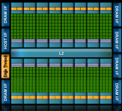
Fermi/GF100 as announced in September of 2009
Before we get too far ahead of ourselves though, let’s talk about what we know and what we don’t know.
During CES, NVIDIA held deep dive sessions for the hardware press. At these deep dives, NVIDIA focused on 3 things: Discussing GF100’s architecture as is relevant for a gaming/consumer GPU, discussing their developer relations program (including the infamous Batman: Arkham Asylum anti-aliasing situation), and finally demonstrating GF100 in action on some games and some productivity applications.
Many of you have likely already seen the demos, as videos of what we saw have already been on YouTube for a few days now. What you haven’t seen and what we’ll be focusing on today, is what we’ve learned about GF100 as a gaming GPU. We now know everything about what makes GF100 tick, and we’re going to share it all with you.
With that said, while NVIDIA is showing off GF100, they aren’t showing off the final products. As such we can talk about the GPU, but we don’t know anything about the final cards. All of that will be announced at a later time – and no, we don’t know that either. In short, here’s what we still don’t know and will not be able to cover today:
- Die size
- What cards will be made from the GF100
- Clock speeds
- Power usage (we only know that it’s more than GT200)
- Pricing
- Performance
At this point the final products and pricing are going to heavily depend on what the final GF100 chips are like. The clockspeeds NVIDIA can get away with will determine power usage and performance, and by extension of that, pricing. Make no mistake though, NVIDIA is clearly aiming to be faster than AMD’s Radeon HD 5870, so form your expectations accordingly.
For performance in particular, we have seen one benchmark: Far Cry 2, running the Ranch Small demo, with NVIDIA running it on both their unnamed GF100 card and a GTX285. The GF100 card was faster (84fps vs. 50fps), but as Ranch Small is a semi-randomized benchmark (certain objects are in some runs and not others) and we’ve seen Far Cry 2 to be CPU-limited in other situations, we don’t put much faith in this specific benchmark. When it comes to performance, we’re content to wait until we can test GF100 cards ourselves.
With that out of the way, let’s get started on GF100.


115 Comments
View All Comments
x86 64 - Sunday, January 31, 2010 - link
If we don't know these basic things then we don't know much.1. Die size
2. What cards will be made from the GF100
3. Clock speeds
4. Power usage (we only know that it’s more than GT200)
5. Pricing
6. Performance
Seems a pretty comprehensive list of important info to me.
nyran125 - Saturday, January 30, 2010 - link
You guys that buy a brand new graphics card every single year are crazy . im still running an 8800 GTS 512mb with no issues in any games whatso ever DX10, was a waste of money and everyones time. Im going to upgrade to the highest end of the GF100;s but thats from a 8800 GTS512mb so the upgrade is significant. Bit form a heigh end ati card to GF 100 ?!?!?!? what was the friggin point in even getting a 200 series card.!?!?!!?1/. Games are only just catching up to the 9000 series now.Olen Ahkcre - Friday, January 22, 2010 - link
I'll wait till they (TSMC) start using 28nm (from planned 40nm) fabrication process on Fermi... drop in size, power consumption and price and rise is clock speed will probably make it worth the wait.It'll be a nice addition to the GTX 295 I currently have. (Yeah, going SLI and PhysX).
Zingam - Wednesday, January 20, 2010 - link
Big deal... Until the next generation of Consoles - no games would take any advantage of these new techs. So? Why bother?zblackrider - Wednesday, January 20, 2010 - link
Why am I flooded with memories of the 20th Anniversary Macintosh?Zool - Wednesday, January 20, 2010 - link
Tesselation is quite resource hog on shaders. If u increase polygons by tenfold (quite easy even with basic levels of tesselation factor) the dissplacement map shaders needs to calculate tenfold more normals which ends in the much more detailed dissplacement of course. The main advatage of tesselation is that it dont need space in video memmory and also read(write ?) bandwith is on chip but it actualy acts as you would increase the polygons in game. Lightning, shadows and other geometry based efects should act as on high polygon models too i think (at least in uniengine heaven u have shadows after tesselation where before u didnt had a single shadow).Only the last stage of tesselator the domain shader produces actual vertices. The real question would be how much does this single(?) domain shader in radeons keep up with the 16 polymorph engines(each with its own tesselation engines) in gt300.
Thats 1(?) domain shader for 32 stream procesors in gt300(and much closer) against 1(?) for 320 5D units in radeon.
If u have too much shader programs that need the new vertices cordinations the radeon could end up being realy botlenecked.
Just my toughs.
Zool - Wednesday, January 20, 2010 - link
Of course ati-s tesselation engine and nvidias tesselation engine can be completly different fixed units. Ati-s tesselation engine is surely more robust than a single tesselation engine in nvidias 16 polymorph engines as its designed for the entire shaders.nubie - Tuesday, January 19, 2010 - link
They have been sitting on the technology since before the release of SLi.In fact SLi didn't have even 2-monitor support until recently, when it should have had 4-monitor support all along.
nVidia clearly didn't want to expend the resources on making the software for it until it was forced, as it now is by AMD heavily advertising their version.
If you look at some of their professional offerings with 4-monitor output it is clear that they have the technology, I am just glad they have acknowledged that it is a desire-able feature.
I certainly hope the mainstream cards get 3-monitor output, it will be nice to drive 3 displays. 3 Projectors is an excellent application, not only for high-def movies filmed in wider than 16:9 formats, but games as well. With projectors you don't get the monitor bezel in the way.
Enthusiast multi-monitor gaming goes back to the Quake II days, glad to see that the mainstream has finally caught up (I am sure the geeks have been pushing for it from inside the companies.)
wwwcd - Tuesday, January 19, 2010 - link
Maybe I'll live to see if Nvidia still wins AMD / Ati, a proposal which is as leadership price / performance, or even as productivity, regardless of price!:)AnnonymousCoward - Tuesday, January 19, 2010 - link
They should make a GT10000, in which the entire 300mm wafer is 1 die. 300B transistors. Unfortunately you have to mount the final thing to the outside of your case, and it runs off a 240V line.