TSMC's 1.6nm Technology Announced for Late 2026: A16 with "Super Power Rail" Backside Power
by Anton Shilov on April 25, 2024 7:30 AM EST
With the arrival of spring comes showers, flowers, and in the technology industry, TSMC's annual technology symposium series. With customers spread all around the world, the Taiwanese pure play foundry has adopted an interesting strategy for updating its customers on its fab plans, holding a series of symposiums from Silicon Valley to Shanghai. Kicking off the series every year – and giving us our first real look at TSMC's updated foundry plans for the coming years – is the Santa Clara stop, where yesterday the company has detailed several new technologies, ranging from more advanced lithography processes to massive, wafer-scale chip packing options.
Today we're publishing several stories based on TSMC's different offerings, starting with TSMC's marquee announcement: their A16 process node. Meanwhile, for the rest of our symposium stories, please be sure to check out the related reading below, and check back for additional stories.
- TSMC's 1.6nm Technology Announced for Late 2026: A16 with "Super Power Rail" Backside Power
- TSMC 2nm Update: N2 In 2025, N2P Loses Backside Power, and NanoFlex Brings Optimal Cells
- TSMC Preps Cheaper 4nm N4C Process For 2025, Aiming For 8.5% Cost Reduction
- TSMC's System-on-Wafer Platform Goes 3D: CoW-SoW Stacks Up the Chips
- TSMC Jumps Into Silicon Photonics, Lays Out Roadmap For 12.8 Tbps COUPE On-Package Interconnect
- TSMC Readies 8x Reticle Super Carrier Interposer For Next-Gen Chips Twice as Large As Today's
Headlining its Silicon Valley stop, TSMC announced its first 'angstrom-class' process technology: A16. Following a production schedule shift that has seen backside power delivery network technology (BSPDN) removed from TSMC's N2P node, the new 1.6nm-class production node will now be the first process to introduce BSPDN to TSMC's chipmaking repertoire. With the addition of backside power capabilities and other improvements, TSMC expects A16 to offer significantly improved performance and energy efficiency compared to TSMC's N2P fabrication process. It will be available to TSMC's clients starting H2 2026.
TSMC A16: Combining GAAFET With Backside Power Delivery
At a high level, TSMC's A16 process technology will rely on gate-all-around (GAAFET) nanosheet transistors and will feature a backside power rail, which will both improve power delivery and moderately increase transistor density. Compared to TSMC's N2P fabrication process, A16 is expected to offer a performance improvement of 8% to 10% at the same voltage and complexity, or a 15% to 20% reduction in power consumption at the same frequency and transistor count. TSMC is not listing detailed density parameters this far out, but the company says that chip density will increase by 1.07x to 1.10x – keeping in mind that transistor density heavily depends on the type and libraries of transistors used.
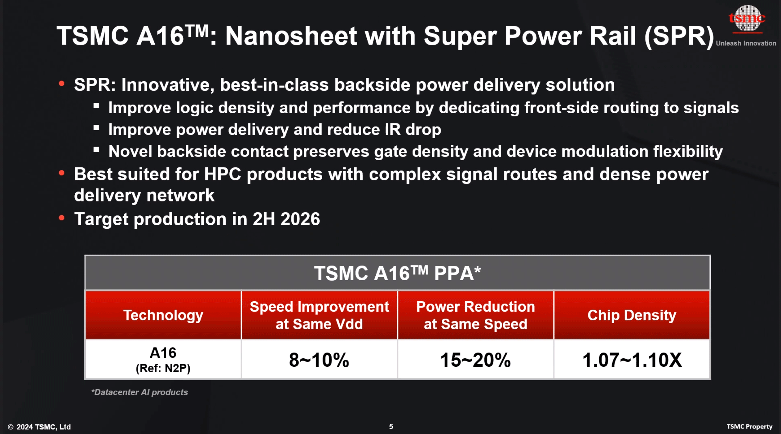
The key innovation of TSMC's A16 node, is its Super Power Rail (SPR) backside power delivery network, a first for TSMC. The contract chipmaker claims that A16's SPR is specifically tailored for high-performance computing products that feature both complex signal routes and dense power circuitry.
As noted earlier, with this week's announcement, A16 has now become the launch vehicle for backside power delivery at TSMC. The company was initially slated to offer BSPDN technology with N2P in 2026, but for reasons that aren't entirely clear, the tech has been punted from N2P and moved to A16. TSMC's official timing for N2P in 2023 was always a bit loose, so it's hard to say if this represents much of a practical delay for BSPDN at TSMC. But at the same time, it's important to underscore that A16 isn't just N2P renamed, but rather it will be a distinct technology from N2P.
TSMC is not the only fab pursuing backside power delivery, and accordingly, we're seeing multiple variations on the technique crop up at different fabs. The overall industry has three approaches for BSPDN: Imec's Buried Power Rail, Intel's PowerVia, and now TSMC's Super Power Rail.
The oldest technique, Imec's Buried Power Rail, essentially places power delivery network on the backside of the wafer and then connects power rail of logic cells to power contact using nano TSVs. This enables some area scaling and does not add too much complexity to production. The second implementation, Intel's PowerVia, connects power to the cell or transistor contact, which provides a better result, but at the cost of complexity.
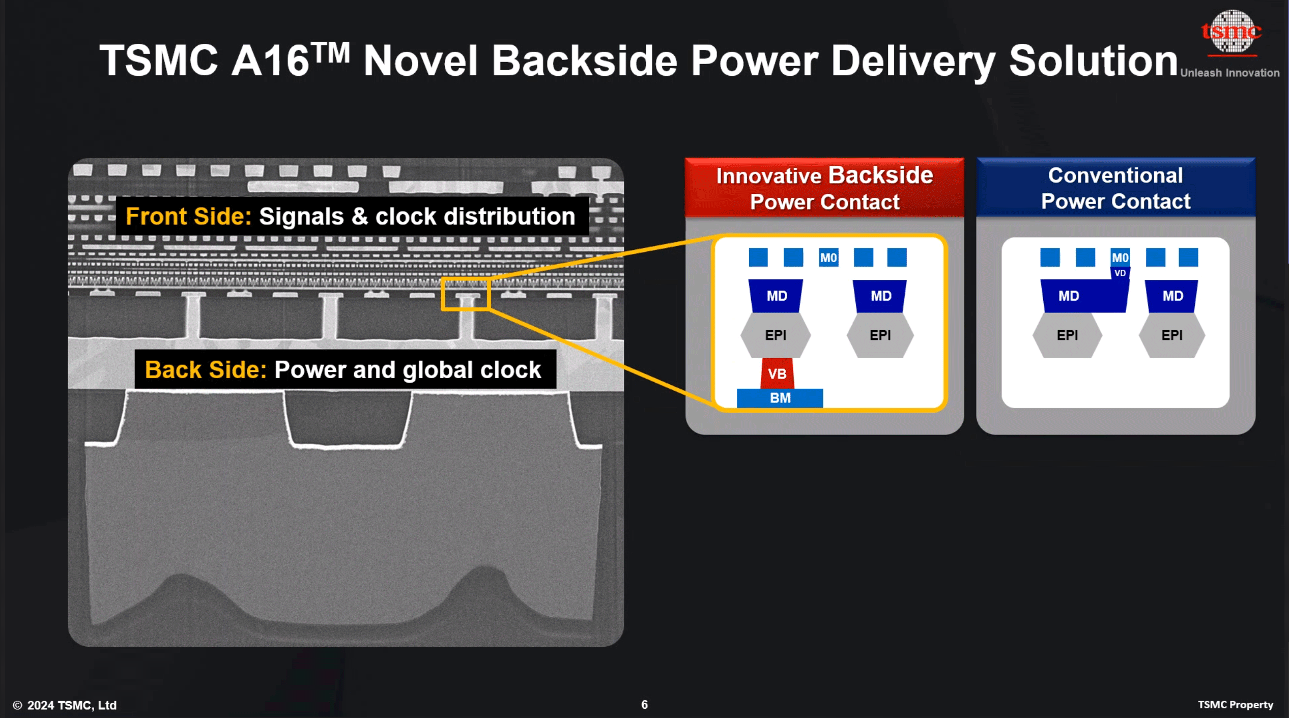
Finally, we have TSMC's new Super Power Rail BSPDN technology, which connects a backside power network directly to each transistor's source and drain. According to TSMC, this is the most efficient technology in terms of area scaling, but the trade-off is that it's the most complex (and expensive) when it comes to production.
That TSMC has opted to go with the most complex version of BSPDN may be part of the reason that we've seen it removed from N2P, as implementing it will ultimately add to both time and costs. This leaves A16 as TSMC's premiere performance node for the 2026/2027 time-frame, while N2P can be positioned to offer a more balanced combination of performance and cost efficiency.
Angstrom Era Kicks Off In Late 2026 With New Node Naming Convention
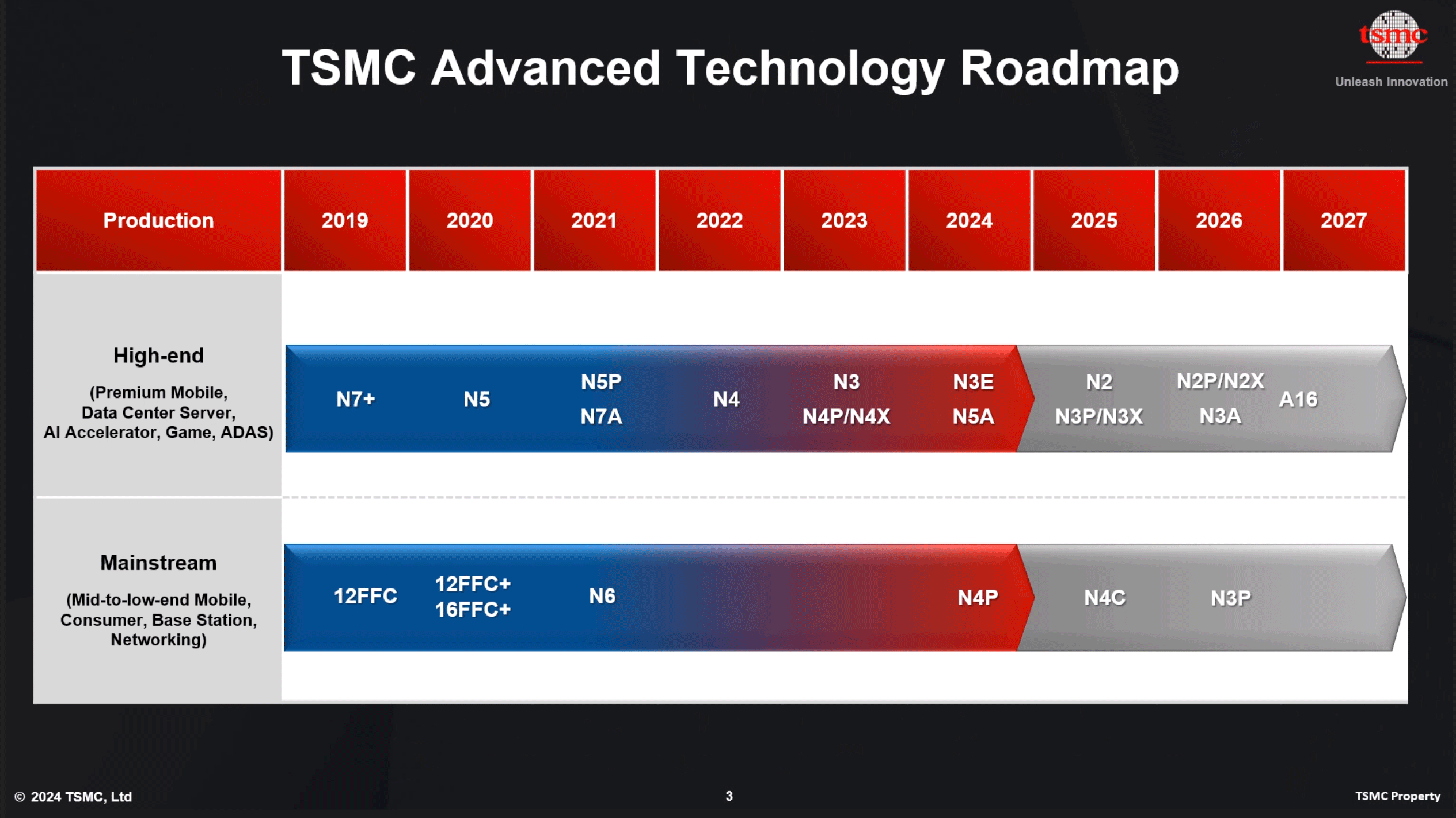
Finally, as with Intel, we're also seeing TSMC adopt a new process node naming convention starting with this generation of technology. The name itself is largely arbitrary – and this has already been the case in the fab industry for several years now – but with current node names already in the single digits (e.g. N2), the industry has needed to re-calibrate node names to something smaller than the nanometer. And thus we've arrived at the 'angstrom era.' But regardless of what exactly it's called or why it's called that, the important point is that A16 will be the next generation node beyond TSMC's 2nm-class products.
TSMC expects to start volume production on A16 in H2 2026, so it is likely that the first products based on this technology will hit the market in 2027. Given the timing, the production node will presumably compete against Intel's 14A; though at 2+ years out and with no one producing BSPDN in volume today, there's still a lot of time for plans and roadmaps to change.


18 Comments
View All Comments
Threska - Thursday, April 25, 2024 - link
Backside Power Delivery is the future although I suspect manufacturing will have to change quite a bit with silicon no longer in the support role.https://youtu.be/hyZlQY2xmWQ
dwbogardus - Friday, April 26, 2024 - link
I have read that thin but solid glass substrates are being considered for the structural support as opposed to the polymer (fiberglass) materials used for many years. They are quite dimensionally stable, and have a TCE similar to silicon. They will need "through-glass vias" for I/O and power to get from the chip to the socket.my_wing - Monday, April 29, 2024 - link
Don't Mix packing to on die with BSPDaccording to Applied Materials presentation the connection point of BSPD is using Tungsten / Cobalt as Cobalt is more rare and from Intel 10nm experience quiet difficult to master, Tungsten as a change is most likely.
https://ir.appliedmaterials.com/static-files/b418f...
name99 - Thursday, April 25, 2024 - link
"But at the same time, it's important to underscore that A16 isn't just N2P renamed, but rather it will be a distinct technology from N2P."I think the elements of this explain what happened.
BSPD requires somewhat more rethinking of chip layout than many previous node improvements (for example I've seen some Apple patents for alternative SRAM cache layouts that exploit BSPD).
My guess is that some customers told TSMC that, rather than having the next upgrade to N2 (ie N2P) based on BSPD, they'd prefer an "easy" optical-shrink-style upgraded node, with BSPD placed on a different track, one that requires a new design rather than a slightly updated design.
ie this is not about "failure" or "slowing down", it's about TSMC being responsive to customers, the same attitude that got them to number one, and that keeps them there. Same reason that there's a "Mainstream" TSMC track with nodes like N4P and N3P that are "easy" upgrades for existing customer designs.
my_wing - Monday, April 29, 2024 - link
What they (CC Wei@TSMC) actually painting the picture is that:TSMC version of BSPD is better than PowerVia@Intel. "Super"
In layman's term BSPD connect power from the backside to 1 of the 3 layers and/or location. (order in terms of performance / complexity)
On top of the silicon i.e. M0 Metal Layer
Same layer of the silicon i.e. PowerVIA
On the bottom of the Silicon i.e. TSMC "Super"
They trying to tell us that because they are "Super" then is Okay, we are "In CC Wei@TSMC" mouth as we are paperly and PowerPoint wise ahead of Intel.
Then they say because we are slow, we gain Qualcomm as their customer. Is okay. From the Intel point of view, Intel actual silver bullet is Intel ARC, as battlemage is coming to launching cycle, Celestial should be is full steam development, if battlemage successfully captured a significant low end market with 10% GP, i.e. my take is that the top battlemage will be 10-15% more expensive as current ARC is losing money, but the driver and everything is going to be improving continuously (Pat was the CEO of VMware, no doubt he can execute here). Then Celestial will be based on Intel 3 E and the SoC will also be based on Intel 3 E, then Intel will leave TSMC (effectively). As an Intel Watcher and as an qualified accountant, I can tell you is that Intel earning estimate always is conservative, take a gain of salt when they say Intel foundry will be money losing for 3 years, more likely in 2026 will breakeven as Celestial Ramp.
name99 - Tuesday, April 30, 2024 - link
Does anyone have a clue what the above is supposed to mean?I think the message is "TSMC sucks, Intel rules", but beyond that I am lost.
my_wing - Wednesday, May 1, 2024 - link
Don't just come in with simple things, like Oh Fanboy, Bias La La La.I already provide with a very simple explanation, where 90% of us is, we are not all earning a living from making semi-conductor.
https://ir.appliedmaterials.com/static-files/b418f...
The presentation is already shared above, should I needed to repeat that and if you look at page 32, to sum it in short is what I have said.
What TSMC is saying is that they are implementing the "Backside Contact to S/D", what CC Wei@TSMC did is that he copy Page 32 of the Applied Material PowerPoint and owned it by comparing the performance of A16 to N2P, which now most of the people outside TSMC thinks N2P will have have any sort of BSPD. And there is no data (technical) to verify what is told.
On the other hand, it is little to no surprise if you signed a non-disclose agreement, you will gain access to Arrow Lake as of now. As they try to paper launch it in Dec 2024.
TSMC@Chang is not suck, it is the best managed company, I personally invested into it and earned 400% return, I also really hope that TSMC will make it. For the greater the love comes with greater the anger. I think, please let Chang come back, take CC Wei Off, as there is none that CC Wei done was really going well, TSMC N3B technically late/failure (off by year), now TSMC "True" N2P is become A16 and push out for another year.
The point is that Bob Swan@Intel, already given you the golden opportunities, not like from 70s to 10s where Intel is always 1-2 nodes ahead, it is good for competition and customer.
CC Wei needed to answer a couple of question to justify his move, the (new) CEO of ASML and CEO of Applied Materials should asked the questions to CC Wei (if not already).
How is your CULitho works, is AI the silver bullet to be the next best thing in Litho?
What is your plan to continuously scale down if CULitho is working?
Will it be better you allow another foundry (except Intel) so that we can work the High EUV NA in, isn't 2030 is just too unreal?
What is your manufacturing plan in Germany, because you suffer so much in the US, do you think that you can handle the added regulation of the EU, e.g. the new Intel German Fab hit ruins site and had to delay until the site is become suitable for construction, does TSMC have the planning as a package to operate outside of Asia?
Each of those is a multi-Billion dollar questions, I don't think CC Wei and the Management of TSMC is answering these.
So it is not TSMC sucks and Intel rules, be honest, I see something, it make sense, the market not make sense, at the end, the market will balance itself out, for those can see a clear picture, will be rewarded, I remember when I invest in TSMC, every big banks is downgrading like crazy in my mind, and at the end, I make 400% profit (ex div), with the company for 5-6 years, not bad.
do_not_arrest - Friday, April 26, 2024 - link
This *could* provide a small opening for Intel. Intel has BSPD in their 2nm-class node, and if they can get some foundry customers now based on the improvements due to that, it will provide those customers an easy migration to their "14A" node which presumably has the same features. On the other hand, now that TSMC has bailed on BSPD for 2nm, it provides THEIR customers an easier path from 4/3 to 2, so they are less likely to lose those customers to Intel. It's very interesting.nandnandnand - Friday, April 26, 2024 - link
Slow and steady vs. Steady delaysmy_wing - Monday, April 29, 2024 - link
Slow and Steady (Pat@Intel) Vs Steady delays (CC Wei@TSMC)Slow and Steday (Chang@TSMC) Vs Steady delay (Bob Swan@Intel)