Next-Gen NVIDIA Teslas Due This Summer; To Be Used In Big Red 200 Supercomputer
by Ryan Smith on January 31, 2020 5:00 PM EST- Posted in
- GPUs
- Tesla
- NVIDIA
- Machine Learning
- Supercomputers
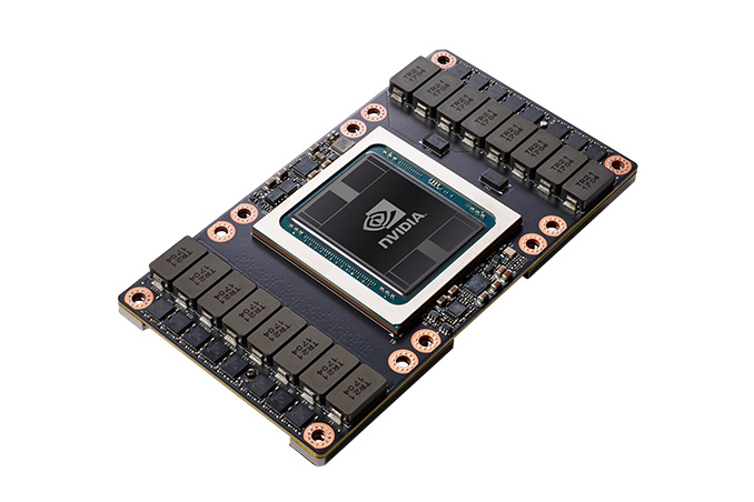
Thanks to Indiana University and The Next Platform, we have a hint of what’s to come with NVIDIA’s future GPU plans, with strong signs that NVIDIA will have a new Tesla accelerator (and underlying GPU) ready for use by this summer.
In an article outlining the installation of Indiana University's Big Red 200 supercomputer – which also happens to be the first Cray Shasta supercomputer to be installed – The Next Platform reports that Indiana University has opted to split up the deployment of the supercomputer in to two phases. In particular, the supercomputer was meant to be delivered with Tesla V100s; however the university has instead opted to hold off on delivery of their accelerators so that they can instead have NVIDIA’s next-generation accelerators, which would make them among the first institutions to get the new accelerators.
The revelation is notable as NVIDIA has yet to announce any new Tesla accelerators or matching GPUs. The company’s current Tesla V100s, based on the GV100 GPU, were first announced back at GTC 2017, so NVIDIA’s compute accelerators are due for a major refresh. However it’s a bit surprising to see anyone other than NVIDIA reveal any details about the new parts, given how buttoned-down the company normally is about such details.
At any rate, according to Indiana University the group expects to have their new accelerators installed by later this summer, with Big Red 200 running in CPU-only mode for now. The Next Platform article goes on to state that the newer accelerators will deliver “70 percent to 75 percent more performance” than NVIDIA’s current V100 accelerators, which assuming it’s accurate, would make for a hefty generational upgrade in performance. Though as always, with multiple modes of compute involved – everything from straight FP32 vector math to tensor operations to low precision operations – the devil is in the details on where those performance gains would most be realized.
In the meantime, NVIDIA’s next GTC event is scheduled for mid-March. So if NVIDIA is planning to launch a new Tesla, then I would certainly expect to see it there.
Source: The Next Platform


38 Comments
View All Comments
quorm - Friday, January 31, 2020 - link
Would this be Turing or Ampere based?Ryan Smith - Friday, January 31, 2020 - link
Officially, we don't know. However given the timing, I would imagine it would be based on NVIDIA's next-gen architecture.SaberKOG91 - Friday, January 31, 2020 - link
I'm going to predict that this will be Ampere, but that Ampere will not see large changes in its design from Turing. It'll be a 7nm die shrink, with PCI-E 4.0 and faster RT performance. The number shaders will probably go up at the highest SKUs. Tensor Cores will be unchanged, but they'll market some new software feature to make them more useful in consumer workloads. And in order to make the launch spicier, Nvidia will announce something related to the display engine, most likely DisplayPort 2.0 or HDMI 2.1.Kevin G - Friday, January 31, 2020 - link
PCIe 4.0 is kinda of a surprise that it isn't active in Turing: Volta supports the PHY speeds for nvLink to POWER9 chips.More ALUs and tensor cores is pretty much a given at the high end but I don't see much of change in the middle. Rather nVidia is just going to reap the rewards of smaller die sizes to boost profit margins while the performance benefits stem mainly from clock speed increases. Recall that the GV100 die is a record holder at 818 mm^2 with the TU102 coming in north of 650 mm^2. Those are stupid large sizes and a die shrink is pretty much necessary to return to yield sanity.
One variable is if the highend still throws a lot of silicon towards compute but follows a chiplet philosophy with it being comprised of more than one die + HBM memory. This would be the more interesting solution in terms of design as the cost penalty has been paid for exotic packaging and design but scales up, very, very well.
I think HDMI 2.1 is a sure thing at this juncture. DP 2.0 is a bit of wild card and may only appear on the last of the chips introduced in this generation. It'd work out in a weird way as the low end chips often get tasked for high resolution digital signage in the professional space.
SaberKOG91 - Friday, January 31, 2020 - link
Just to be clear, Tensor Cores don't exist as separate logic. They are just groups of 8 shaders being used together to carry out operations more efficiently than if they were doing the same calculations as individual instructions. Same thing goes for RT cores. They are just lots of shaders working together with a little bit of extra logic to carry out BVH efficiently.We won't see MCM for Ampere, that won't come until Hopper.
p1esk - Friday, January 31, 2020 - link
> Tensor Cores don't exist as separate logicDo you have a link to back that up? You might be right, but I can't find it in Nvidia docs.
Yojimbo - Saturday, February 1, 2020 - link
NVIDIA isn't going to public its trade secrets.Yojimbo - Saturday, February 1, 2020 - link
I think you went too far from the one extreme (believing the cores were entirely separate new blocks of transistors) to the other (seeming to believe that the addition of the tensor cores and RT cores is more or less trivial). Most likely the tensor cores are made by giving the shaders alternate, specialized data pathways to make efficient macro operations. But we don't know that for sure. As far as the RT cores, they haven't been around as long and I think even less is known about them. Ideally NVIDIA would want to reuse as much of the compute cores as possible. But, to my understanding, incoherent rays present a big problem for the standard data pathway of SIMD/SIMT hardware. The key thing for both the tensor cores and the RT cores are the data pathways: reducing the I/O bandwidth. But that is the key part of the engineering of the SIMT hardware, as well. It's relatively extremely easy to build number-crunching MAC units. It can be done cheaply and quickly with just a few engineers, as seen by all the AI chip startups and Tesla. But building a GPU that is able to efficiently use those units for general purpose compute in an offload model is a much bigger engineering challenge. The same can be said for the tensor cores and the RT cores. Those data pathways ARE the heart of the cores. They aren't just "a little bit of extra logic".SaberKOG91 - Saturday, February 1, 2020 - link
I spent a lot of time reading up on it after our back and forth and found various developers talking about their experiences with Turing on Reddit and other places. These are folks who actually spend the time tracing wavefronts as they are scheduled and staring at assembly code. Their experience changed my mind, which happens occasionally :p These folks have been able to confirm that you can't use Tensor Cores and vanilla CUDA Cores simultaneously which pretty much proves that Nvidia is breaking each SM into 8 groups of 8 shaders, with each group able to be configured as a Tensor Core. As far as RT cores are concerned, they have also been able to confirm that using and RT at all means that the entire SM becomes unavailable for other operations. They also insist that there are new instructions for BVH that would require new hardware. BVH is the part of RT that can't efficiently be calculated by FP operations. Nvidia are using optimized hardware to do the BVH traversal and then using a compressed form of the traversed path to determine the sequence of vector transforms that are necessary to get from the source to the camera. The transforms and any subsequent application of material properties, are all SIMD optimized tasks. BVH relative to the rest of the computational resources within an SM is a tiny fraction of the area that is distributed across groups of shaders. Not some huge chunk like the Nvidia marketing material would have you believe. This is all smoke and mirrors, hiding the fact that Nvidia's approach to ray-tracing is actually quite similar to the one AMD has proposed where they also use the shaders for the bulk of the computation and use other hardware resources to perform the BVH.Yojimbo - Saturday, February 1, 2020 - link
Informative. The information on the compressed BVHs can be found in a 2017 NVIDIA research paper, BTW. But there is no guarantee that that is what Nvidia are using. I am skeptical that anyone can know because the underlying operations are not exposed. Did those forums explain exactly how they could determine that?I also think it's inappropriate both to call it smoke and mirrors and to say it is the same as an implementation that we have even less information on (AMD's).
I don't think we know how much space the RT cores take up, and I don't think NVIDIA ever claimed any percentage of die space. People took Nvidia's schematics as representing relative die areas. I have argued with various people about that since Turing was introduced. I never took those schematics as meaning to be representative of die areas and I'm not sure why people did. I mean, look: https://images.anandtech.com/doci/13214/Turing_575...
Would the NVLink block look just like the decode block, just like the tensor cores, etc? Then there were also the colored ones which were drawn as 1/3,1/3,1/3 of SMs, tensor cores, and RT cores. They were just meant to highlight features in an appealing way. They were never meant to give insight on the workings or layout of the chip or to make any claims of die area.
Various parts of the chip likely need to be changed in order to accommodate what are almost certainly different memory access patterns. Perhaps they need a more general solution, or multiple pathways, changes in the cache, etc. Additionally, it will probably be 4 years between when NVIDIA introduced tensor cores and when AMD have an equivalent. If they were smoke and mirrors then AMD wouldn't have let their AI opportunities wallow in the mud for such a long time.