Hands on with the 56-core Xeon Platinum 9200 CPU: Intel’s Biggest CPU Package Ever
by Ian Cutress on April 8, 2019 11:00 AM EST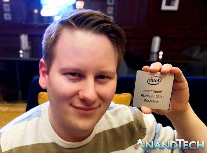
When Intel announced the new Cascade Lake family as officially launched last week, it added a new product segment to its portfolio – the ‘Advanced Performance’ or AP. These come in the form of the Xeon Platinum 9200 family, and feature two of Intel’s high-end processors within a single package, offering double the cores and double the memory in a much denser environment. These processors are focusing purely on density, and are BGA only so they will only be sold as complete systems by OEMs, who actually buy them from Intel and make modifications. We had the opportunity to hold one of these big CPUs and take some pictures.
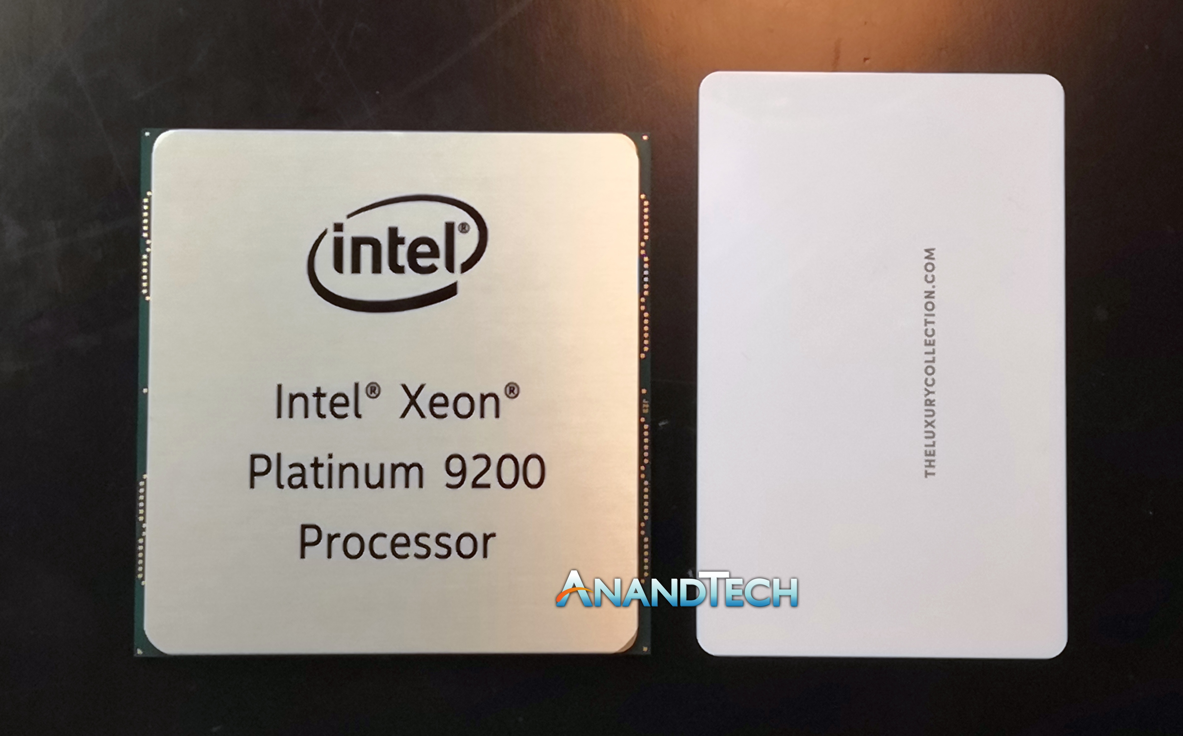
The package measures 76.0 x 72.5 mm, making it Intel’s largest CPU based* package ever, beating out the old Intel Pentium Pro, which was 67.6 x 62.5 mm, and AMD’s EPYC package, which is 75.4 x 58.5 mm.
Source: Intel
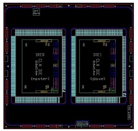
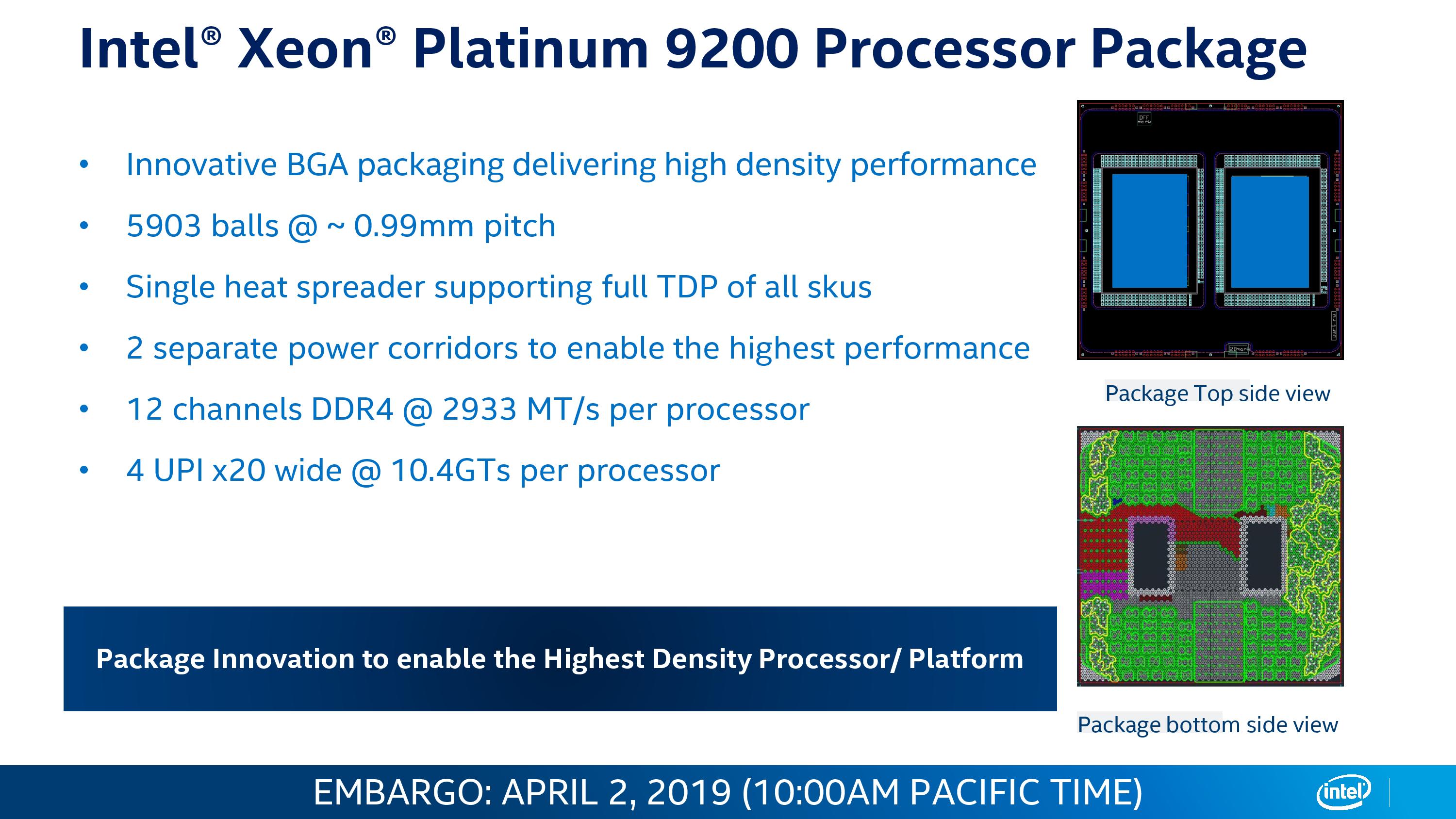
Inside the package is two XCC enabled silicon die, one designated a master, and one a slave. The die themselves are ~694mm2 each.
The Biggest Baller In The Park
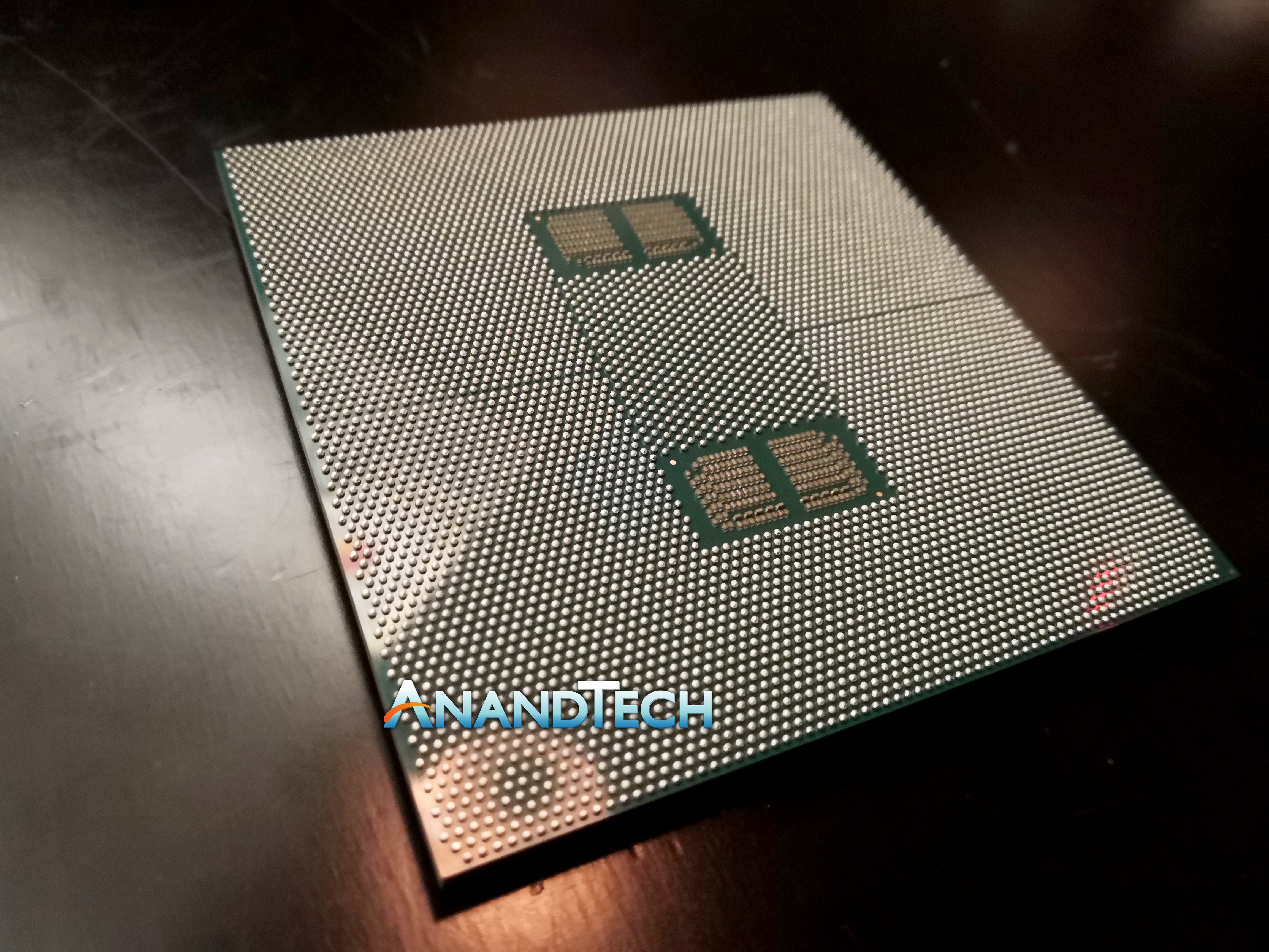
The socket is officially called FCBGA5903, which stands for flip-chip ball-grid array 5903, with 5903 being the number of contacts or ‘balls’ on the underside which goes onto the motherboard, much like an embedded chip. By contrast, AMD’s EPYC chip has 4094 pins. The reason for all these contacts are mostly in the memory: as this Platinum 9200 processor has twelve memory channels, these all require pins. There are also some more for power, as the TDP for the 56-core version is 400W.
To begin, Intel is offering four different types of Platinum 9200:
| Intel Xeon Platinum 9200 Family (Cascade Lake AP) |
||||||
| AnandTech | Cores | Base Freq |
Turbo Freq |
L3 Cache |
TDP | Price |
| Platinum 9282 | 56 C / 112 T | 2.6 GHz | 3.8 GHz | 77.0 MB | 400 W | head |
| Platinum 9242 | 48 C / 96 T | 2.3 GHz | 3.8 GHz | 71.5 MB | 350 W | shoulders |
| Platinum 9222 | 32 C / 64 T | 2.3 GHz | 3.7 GHz | 71.5 MB | 250 W | knees |
| Platinum 9221 | 32 C / 64 T | 2.1 GHz | 3.7 GHz | 71.5 MB | 250 W | toes |
In terms of weight, the processor is definitely around 200-300g, or half a pound. This was measured very scientifically by comparing it in my hands to the weight of my heaviest phone, and then comparing it to two phones. The chip certainly has some hefty bulk, but given that it is a BGA design, it’s unlikely that even people using the chip will ever hold it.

If we look side on to the design, we can see that the package actually has three distinct layering stages (five, if you include the caps). The light brown and dark brown layering totals up to 18 layers (recorded by eye, hard to see in difficult light), and the dark brown layers are clearly double the thickness of the light brown layers, which might indicate that these are the power planes of the package. Normally we see processors with anywhere from 8-12 layers total, so this is another step up above that.

A close up of the ball array shows the fine pitch between the contacts. The capacitors on the underside are extremely tiny in comparison to other CPUs - I mean really small. Each of these corners has 87 capacitors, making for a total of 348.
Pricing for this family of processors is not expected to be disclosed. Intel has stated that as they are selling these chips as part of barebones servers to OEMs that they will unlikely partition out the list pricing of the parts, and expect OEMs to cost them appropriately. Given that the new high-end Intel Xeon Platinum 8280L, with 28 cores and support for 4.5 TB of memory, runs just shy of ~$18k, we might see the top Xeon Platinum 9282 be anywhere from $25k to $50k, based on Intel margins, OEM margins, and markup.

nom nom nom, chips
*Intel may have FPGA products that exceed this size, mainly due to HBM and other chiplets on board.


Related Reading
- Intel's Enterprise Extravaganza 2019 Roundup
- Intel Xeon Scalable Cascade Lake: Now with Optane!
- Intel Agilex: 10nm FPGAs with PCIe 5.0, DDR5, and CXL
- Intel Columbiaville: 800 Series Ethernet at 100G, with ADQ and DDP
- Intel Launches the Xeon D-1600 Family: Upgrades to Xeon D-1500
- Lenovo’s New Cascade Lake ThinkSystem Servers: Up to 8 Sockets with Optane
- Dell PowerEdge Updates: Upgrade to Cascade Lake and Optane
- Supermicro Calvinballs Into Cascade Lake: Over 100 New and Updated Offerings


66 Comments
View All Comments
eva02langley - Monday, April 8, 2019 - link
Cascade Fail...Chaitanya - Monday, April 8, 2019 - link
That's what happens after 10 years of rehashing same architecture.eva02langley - Monday, April 8, 2019 - link
I have read somewhere that these are not modular. Basically, if the mobo die, you need to buy a new board and another CPU.I don't remember where I read this.
Ian Cutress - Monday, April 8, 2019 - link
These are BGA. Soldered onto the motherboard. Intel is selling them as barebones systems to OEMs.Santoval - Monday, April 8, 2019 - link
BGA means soldering. I strongly doubt the CPUs could be unsoldered by the OEMs but it's possible Intel can do it if either the motherboard or the CPU dies. "Can do it" does not equate with "will do it" though. If this occurs in a tiny subset of the parts, and they are within warranty, Intel might just replace the entire thing rather than bother to have some of their technicians do (very carefully) the unsoldering, unpasting etc I am not sure what they would do if the warranty has expired though. It would probably depend on the OEM.Klimax - Thursday, April 11, 2019 - link
There are companies that can do BGA replacement. But not cheaply, especially for such massive BGA as is this case.bobhumplick - Monday, April 8, 2019 - link
if you believe that then get a 10 year old cpu and game on it. go ahead and get a 2080 ti. ill wait.if thats the case i wonder how they got away with it? i mean surely they had a competitor during those 10 years right? cause if so how can you blame intel when the competition still lost to them.
reinventing the wheel can cause problems too. like p4 and fx. both relied on programmers to rewrite code to take advantage of parralellism years before the code was written (p4 with new sse and HT and fx with a bunch of slow cores). iterations are what work. intel hasnt been rehashing the same arch for 10 years. theyve been doing if for 20. and winning mostly.
now amd is back and im glad. but they are back with what? essentially a reverse engineered i7 quad core, doubled up in a dual socket config, then shrunk down to fit it all on one package to cut costs and more importantly latency.
so now even AMD are rehashing intels "old" arch.
intel should have went to 6 cores by the 6th gen at the latest. and they should have decoupled the arch improvements in cannonlake and later icelake from 10nm years ago so it would have worked on 14nm. but they didnt. they stood there like a deer in the headlights for 3 years or so saying "well at least amd still cant compete" until they waited till the that amd could compete with them. they really screwed some things up. but they are taking the right steps to fix it. they are doing things that id never think intel would do. like reaching out to the press and bringing in outsiders (intel never did that before). will it be enough? who knows.
but really intel only started screwing up about 3 years ago. and they kinda bought time with the 8th gen at least. so its more like 2 years maybe. its not insurrmountable. but its gonna take some hussle. and amd aint sleeping for sure
FreckledTrout - Monday, April 8, 2019 - link
Going back 10 years may be a bit far but over 8 years ago the 2500K was released. It still holds its own today when overclocked.Samus - Tuesday, April 9, 2019 - link
While the CPU's hold their own (technically even a i7-920 overclocked to 3.5GHz is competitive) the platforms have huge limitations and make the CPU's irrelevant for most modern applications, especially gaming, especially the ancient PCIe 2.0 bus (which is, per lane, half the speed of 3.0) which on paper might not seem bad since a modern video card at PCIe 3.0 x8 isn't totally saturated so theoretically a PCIe 2.0 x16 should be fine, all things being equal.But then you get into the platform interconnects. The CPU is connected to the northbridge over QPI - the PCIe bus isn't native to the CPU internals, and it gets worse. The northbridge and southbridge are connected over DMI. That's 2GB/sec. The southbridge has ALL other PCIe lanes (like all the x1 lanes) and the SATA and USB controllers, etc. BTW, those native SATA controllers are 3Gbps, not even SATA 3.0, and obviously USB 3.0 wasn't native on an Intel chipset until Haswell (I think, maybe is was on the 70-series natively?)
Basically the platforms sucked until Haswell, and even still 80/90-series mostly lacked m2 NVMe or SATA Express. Some later boards have m2 NVMe PCIe x2 slots, but as far as I know none had x4 and most were never even made bootable because BIOS support sucked from most vendors.
Architecturally, still, you'd be crazy to game on anything older than Haswell. The power efficiency of the platform improved so much (which is why you suddenly saw ITX go mainstream with H\Z87) not just in the CPU but the PCH (shrunk from like 65nm to 32nm cutting power usage IN HALF.) And so many new instructions came around that generation, specifically AVX which is actually required for many games now, and anything DirectX12 requires it since its part of the API.
Alexvrb - Monday, April 8, 2019 - link
"now amd is back and im glad. but they are back with what? essentially a reverse engineered i7 quad core"Nice try. The lead designer of the Zen architecture was Keller, who was also behind the DEC Alpha 21164/264, K7, and K8, and that's just his desktop work. Zen is the successor to those architectures, AMD lost their way with BD et al. Just as Intel did with Netburst. Both of them went back and modernized older designs (Intel used the P6-derived Pentium M as the basis for Core).
Now he works for Intel... they didn't hire him because he made a reasonable facsimile of their architecture.