Quick Note: NVIDIA’s “Einstein” Architecture Was A Real Project
by Ryan Smith on March 19, 2019 12:30 AM EST
While it was never an official NVIDIA codename as far as roadmaps go, the name “Einstein” came up in rumors a few times earlier this decade. At the time, Einstein was rumored to be the architecture that would follow Maxwell in the NVIDIA lineup. And while we sadly didn’t find out anything new about NVIDIA’s future roadmap at this year’s show – or any sign of Ampere or other 7nm chips – I did inadvertently find out that the rumors about Einstein were true. At least, from a certain point of view.
While talking with NVIDIA’s research group this morning about some of their latest projects (more on this a bit later this week when I have the time), the group was talking about past research projects. And, as it turns out, one of those former research projects was Einstein.
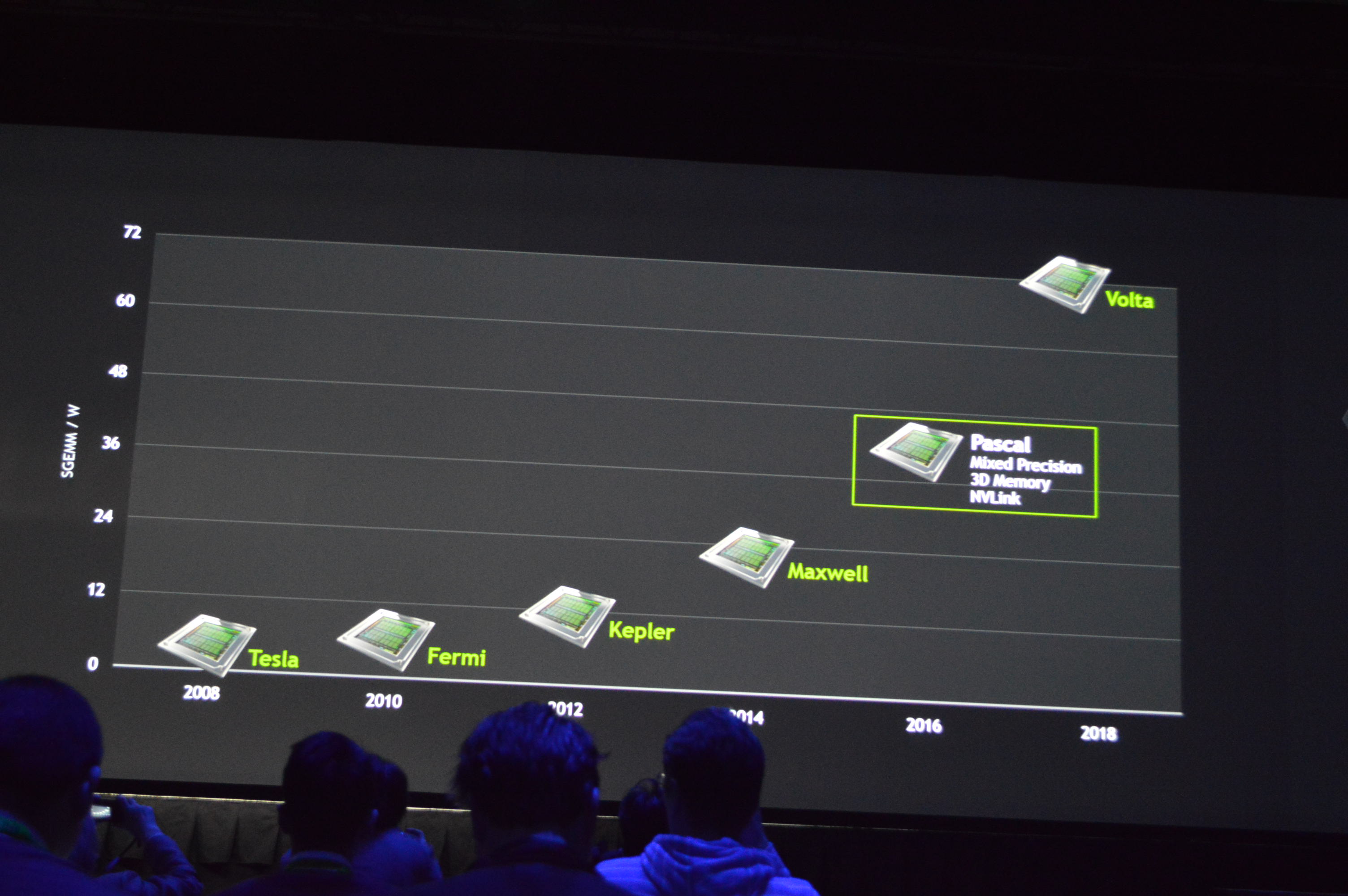
Rather than just being a baseless rumor, Einstein was in fact a real project at NVIDIA. However rather than being an architecture, per-se, it was a research GPU that the NVIDIA research group was working on. And although this research project didn’t bear fruit under the Einstein name, it did under another name that is far more well-known: Volta.
So while this means we can scratch Einstein off of the list of names for potential future NVIDIA architectures, the project itself was real, and it was actually a big success for NVIDIA. As Einstein morphed into what became the Volta architecture, it has become the cornerstone of what are now all of NVIDIA’s current-generation GPUs for servers and clients. This includes both regular Volta and it’s graphics-enhanced derivative, Turing.


15 Comments
View All Comments
R0H1T - Tuesday, March 19, 2019 - link
It's a good thing they didn't go with Einstein, I feel the Einstein–Rosen bridge would've been been too big (far?) to cross 🙃slashclee - Tuesday, March 19, 2019 - link
And people thought Turing's power consumption was high... imagine how much power you'd need to bring up THAT bridge.edzieba - Tuesday, March 19, 2019 - link
Given that even theoretical frameworks for stabilisation of an E-R bridge required negative-mass matter ('negative energy'), maybe it would have a negative TDP?FreckledTrout - Tuesday, March 19, 2019 - link
Depends on which side of the bridge you are measuring from. :)vithrell - Tuesday, March 19, 2019 - link
It would be killer name for Intel-Nvidia setup with Einstein based GTX and Rosen Bridge based i7, tho. ;)HStewart - Tuesday, March 19, 2019 - link
Rosen Bridge would be cool name for Lakefield chipset - with Fovores technology, it could be put on the 3d chip.Kevin G - Tuesday, March 19, 2019 - link
While Einstein eventually morphed into Volta, what made it different? What were the research goals of that project? Why was Einstein dropped? 20 nm?If we have an architecture that never left the lab, what others are lurking? Hawking? Newton? Euler? Schrodinger (though I suspect that will both be released and never see the light of day)?
Speaking of research work and code names, did they let slip what was nVidia's chiplet research project called?
https://research.nvidia.com/publication/2017-06_MC...
CiccioB - Tuesday, March 19, 2019 - link
Yes, it would be really interesting knowing what they are working on for the future.But, alas, we are not allowed to know.
With the acquisition of Mellanox I expect nvidia to create a multi chip GPU soon (probably after the next architecture) based on a highly optimized bus.
That would allow them to overcome the die space limitations (and costs) that are affecting their strategy for increasing GPU functionalities beyond the simple (now quite obsolete) rasterization capabilities.
Kevin G - Tuesday, March 19, 2019 - link
nVidia is in need of updating Volta but a straight shrink to 7 nm may not be feasible at the moment. It takes a bit of time to ramp up to the large monolithic die sizes nVidia leverages. at 818 mm^2, GV100 is the largest mass produced chip ever. A straight shrink to 7 nm would bring it down roughly to the 450 mm^2 which is still a big chip. Any sort of tangible improvement would have to come from a slight up tick in functional units (bringing the chip size north of 500 mm^2) and higher clocks. A >500 mm^2 chip on 7 nm may not yet be feasible in terms of yield (yet). We could be seeing such a chip at the end of this year.More feasible since nVidia apparently has already done some research into this area would be the chiplet idea. Again, I would only expect product at the end of the year but they could feasible use four 400 mm^2 7 mm dies and easily exceed current Volta.
mode_13h - Tuesday, March 19, 2019 - link
They already had two generations of NVLink, as a multi-chip communication framework.Mellanox was probably more about countering Intel's growing dominance of the HPC stack.