IBM And Everspin Announce 19TB NVMe SSD With MRAM Write Cache
by Billy Tallis on August 6, 2018 3:55 PM EST- Posted in
- SSDs
- Storage
- Enterprise SSDs
- IBM
- NVMe
- Everspin
- MRAM
- MRAM Developer Day
A new generation of IBM's FlashSystem storage appliances will be adopting a new architecture with magnetoresistive RAM (MRAM) write caches instead of capacitor-backed DRAM. MRAM is one of the fastest and highest-endurance nonvolatile memory technologies currently available, but it has severely limited density compared to NAND flash memory or Intel's 3D XPoint memory. Until recently, most applications of MRAM were in embedded systems where MRAM could replace small flash chips or battery-backed DRAM and SRAM buffers.
Everspin, the only current supplier of discrete MRAM chips, has been pushing capacities higher with their currently available 256Mb chips and 1Gb chips that will be sampling by the end of this year. This is being enabled by their migration from in-house manufacturing on wafers fabbed at Freescale to a partnership with GlobalFoundries to make MRAM on their 22nm FD-SOI process. These capacity increases have made MRAM more attractive for use in systems that deal with a high volume of data, even though they are still far too small to be used as primary storage.
IBM's existing FlashSystem appliances have used custom form factor SSDs and a system-wide power loss protection design, along with FPGA-based controllers. The new system switches to a standard 2.5" U.2 drive form factor, which requires implementing power loss protection at a per-drive level. IBM found it impractical to include enough supercaps to keep the FPGA controller running long enough to flush their DRAM write caches, but the inherent nonvolatility of MRAM eliminates the need for any bulky supercaps.
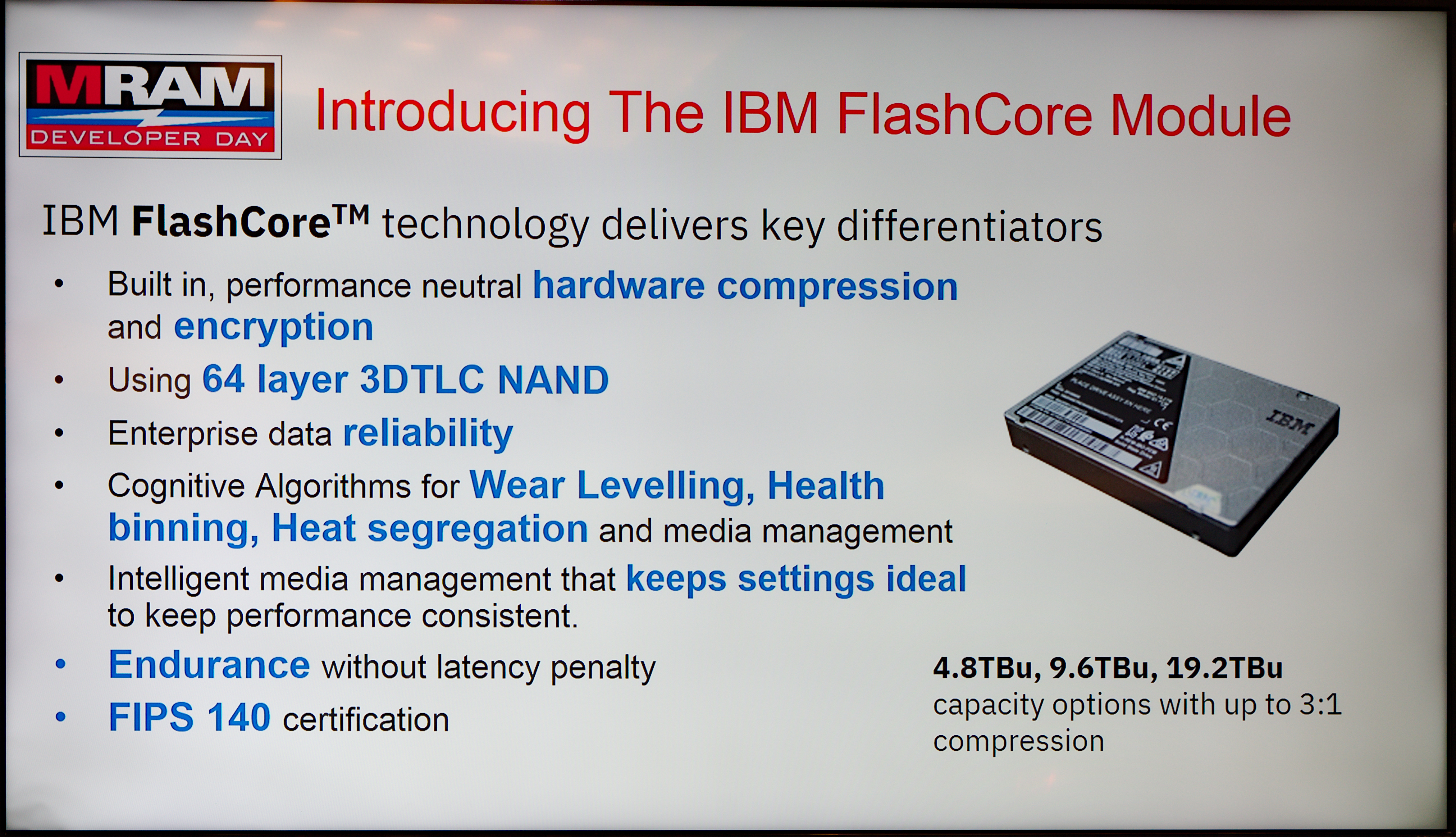
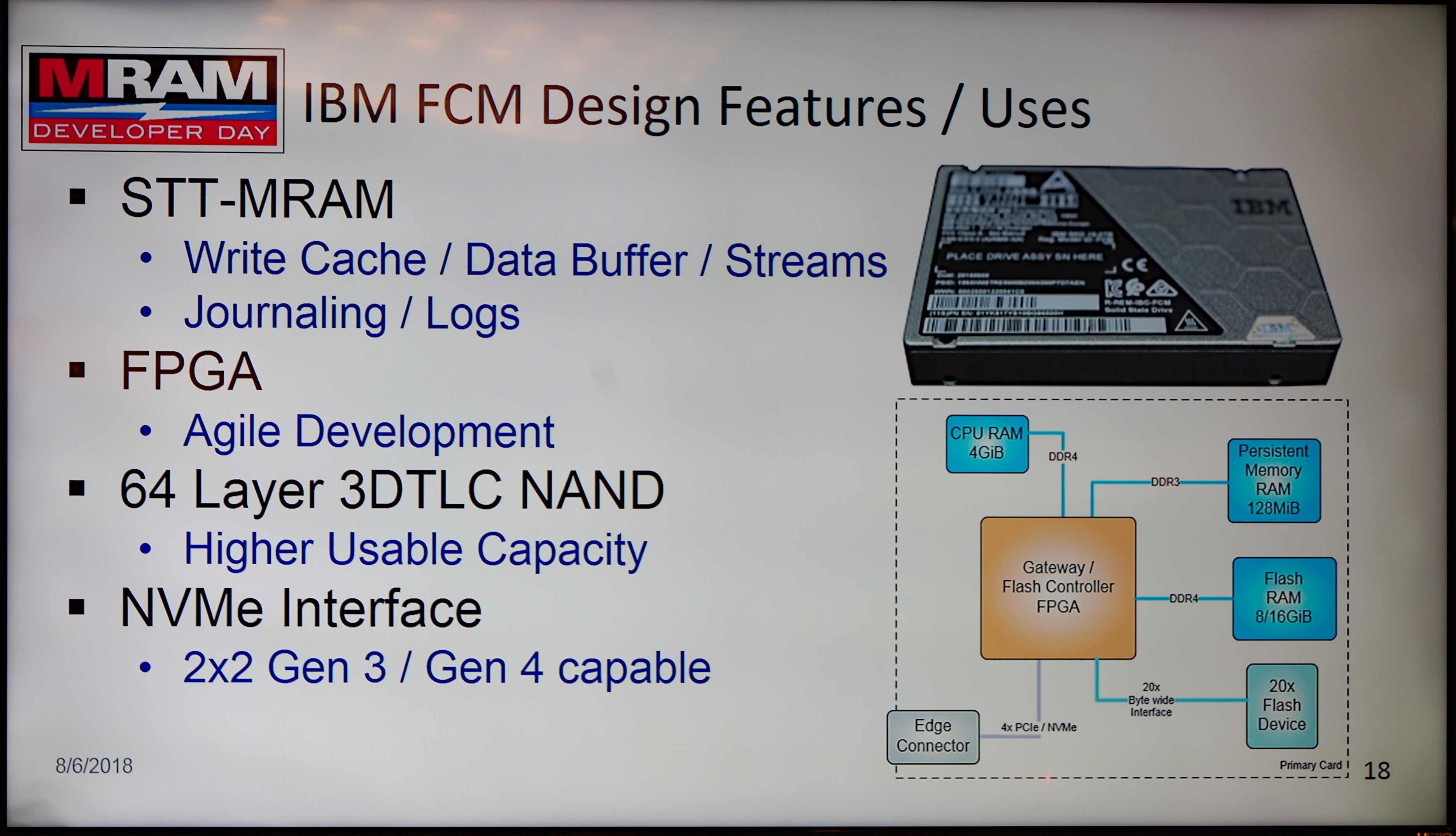
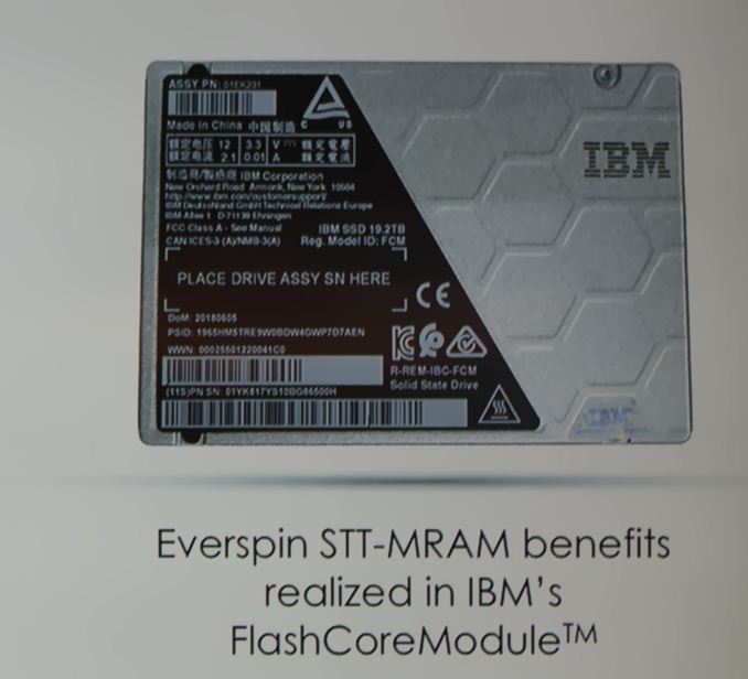
The new SSDs for IBM's FlashSystem have a usable storage capacity of up to 19.2TB of 64L 3D TLC NAND flash memory, making them some of the highest-density TLC-based drives. The drives use a 20-channel NAND interface and a four-lane PCIe 4.0 host interface that can operate in dual-port 2+2 mode. IBM's controller also provides optional transparent compression with a typical 3:1 compression ratio, and FIPS 140 compliant encryption. The new FlashSystem drives will be on display this week at Flash Memory Summit and will be shipping to customers this month.


14 Comments
View All Comments
abufrejoval - Monday, August 6, 2018 - link
Seems more like a PoC than a product. The real MRAM benefit as I understand it is that you can mix logic IP blocks and NV-RAM into a single SoC, which is very low power, very quick to recover its full logic state from MRAM, so it wakes up and resumes in a few dozen cycles: Energy benfits, not space benefits.Here an FPGA with a pure MRAM memory chip will save space where U.2 obviously carries over a spinning rust form factor not ideal for solid state storage.
At current premiums I'm not convinced U.2 will ever flourish and the Open Compute guys will probably cook up something more sensible, quite possibly MRAM based, but not U.2 with FPGA, but a proper ASIC or a set of them for aggregation.
The Hardcard - Monday, August 6, 2018 - link
Not even the “shipping to customers this month” makes it seem like a product?abufrejoval - Tuesday, August 7, 2018 - link
You're right, it's an IBM product. I guess what I was trying to express is that I don't see this as a template for widespread adoption, not this controller and not U.2. It is bleeding edge (as is 19TB in a single SSD), but very niche.Widespread for me means large volume, which is cloud and consumer, not enterprise. We still have a mainframe, we still have p-Series and we have U.2 disks and SSDs where I work.
But we don't have that many.
When I want through the presentation I felt that those hybrid HDDs could now get the cache thay would have requried to make sense (instead of 8GB of SLC being sold at outrageous prices and little value) as part of the normal controller they already need, but those are gone from notebooks and not coming back. 'normal' SSDs could also profit, but SLC chaches seem to work well enough for most cases, so that it would be difficult to compete. And those notebooks typically have a UPS built-in ;-)
Don't get me wrong, I love the technology, but I'm not sure this is the greatest showcase towards mass adoption.
Manch - Tuesday, August 7, 2018 - link
Is it too hard to just type "HDD"?abufrejoval - Tuesday, August 7, 2018 - link
sorry, I read theRegister.co.uk before I look at Anandtech for time zone reasons: It colours off...Ammaross - Tuesday, August 7, 2018 - link
+1 for El Reg. Spinning Rust is the only way to talk about an HDD. :)fteoath64 - Tuesday, August 7, 2018 - link
Noting said about read and write speeds ?. Event preliminary numbers will provide indicative performance compared to normal SSDs.Santoval - Wednesday, August 8, 2018 - link
How much MRAM does this use, 1 Gb (128 MB) or more? Or is it even less, since apparently 1 Gb MRAM hasn't even started sampling yet? What is the real benefit of replacing DRAM cache with a very small MRAM cache apart from saving on supercapacitors, but at the very large trade-off of the cache filling much more quickly?a1exh - Wednesday, August 8, 2018 - link
That was exactly what I was thinking. A traditional map table for a 20TB drive would take approx 32GB of DRAMabufrejoval - Wednesday, August 8, 2018 - link
But would you store a map table in MRAM? AFAIK you can reconstruct the map table from the on flash structures: Yes it would take time, but enterprise hardware typically doesn't get powered off until its going to the knackers and for the rare powerfail event the reconstruction time may not be crucial enough to keep it there. I would have thought that MRAM here is used for crucial in-transit data and base data structures required to reconstruct any map.That's one reason more I don't think this use case is an ideal demonstrator for MRAM, which to my knowledge tried to focus more on really logic embedded SRAM replacement, where complex logic state say in massive DSP or SoC could be persisted very quickly, so sleep/wakeup times could be minimized and the energy expense for the transition reduced to reduce the cost of sleeping. That's IoT, ultra embedded etc. but not high-end ent