The Crucial MX500 500GB SSD Review: A Second Look
by Billy Tallis on February 2, 2018 9:30 AM EST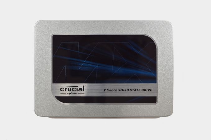
In December, the 1TB Crucial MX500 impressed us with its combination of great performance for a SATA drive and an aggressive introductory price. Since then, Micron has launched the rest of the Crucial MX500 product line, and several other new SSDs have been announced. The most important new competitors aren't any of the many drives shown at CES, but the new Samsung 860 PRO and 860 EVO that launched last week. So far, we have only tested the premium Samsung 860 PRO, but it is clear that the improvements from Samsung's 64-layer 3D NAND process and their updated SATA SSD controller will affect where the 860 EVO stands. The handful of performance records set by the 1TB MX500 didn't last long.
The MX500 is the first Crucial drive based on Micron's 64-layer 3D TLC NAND, and is the second generation of Crucial's mainstream MX series to use TLC NAND instead of MLC NAND. The MX500 breaks from previous MX generations by using Silicon Motion's SM2258 controller instead of a Marvell controller, but all the usual features of the MX series are still present. This includes both TCG Opal encryption support and Crucial's partial power loss protection, features which are uncommon on mainstream or budget consumer SSDs. As usual for Crucial, the SLC write cache is dynamically sized based on how full the drive is.
The Crucial MX500 uses Micron's 256Gb 64L 3D TLC part and consequently returns to the standard drive capacities and overprovisioning ratios, instead of the unusual configurations caused by the 384Gb die capacity in the MX300's 32L 3D TLC. The slightly lower usable capacities of the MX500 than the MX300 means the new drives have slightly higher prices on a per-GB basis, but the MSRPs are still very competitive against current street prices for the competition.
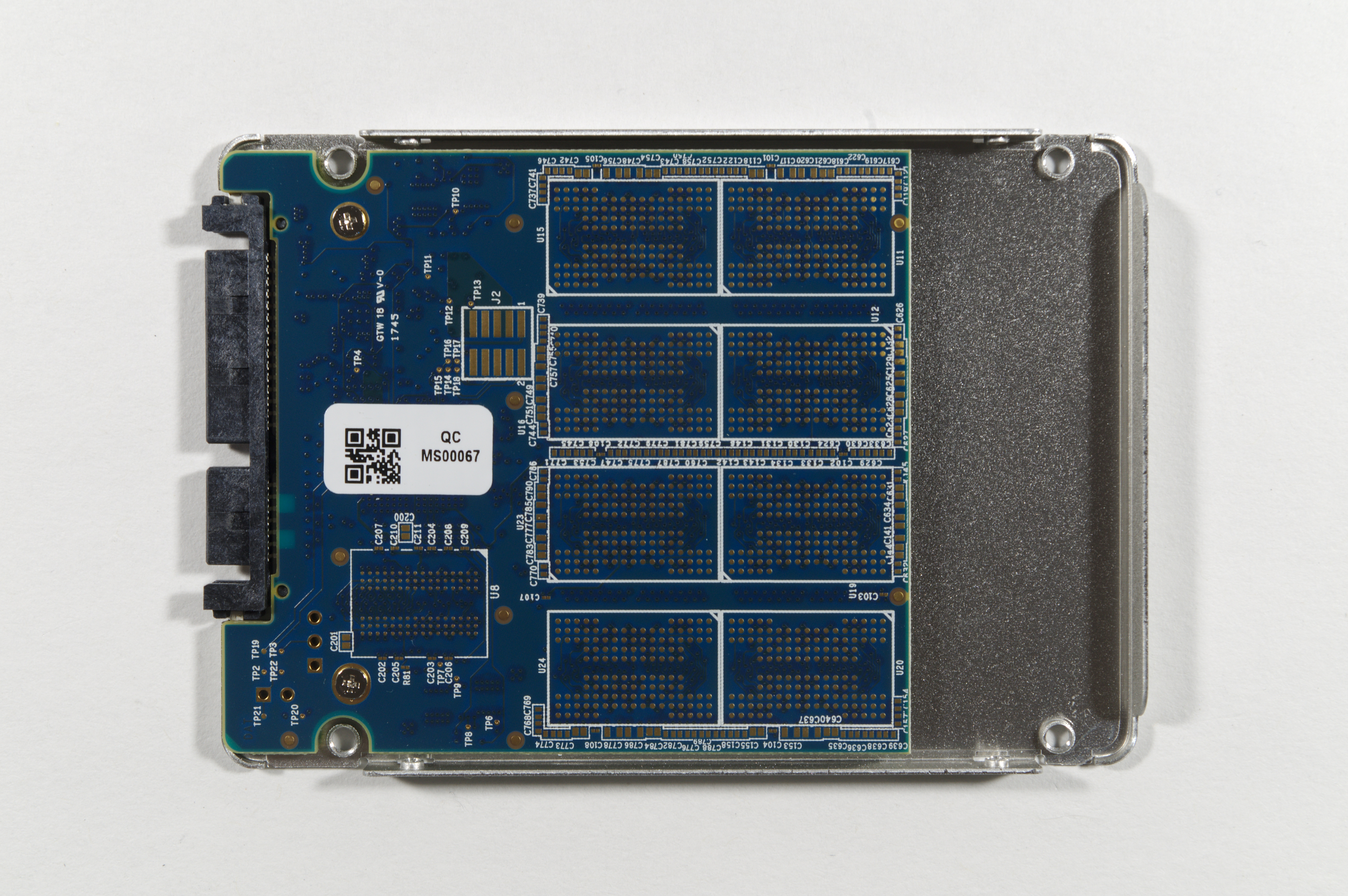
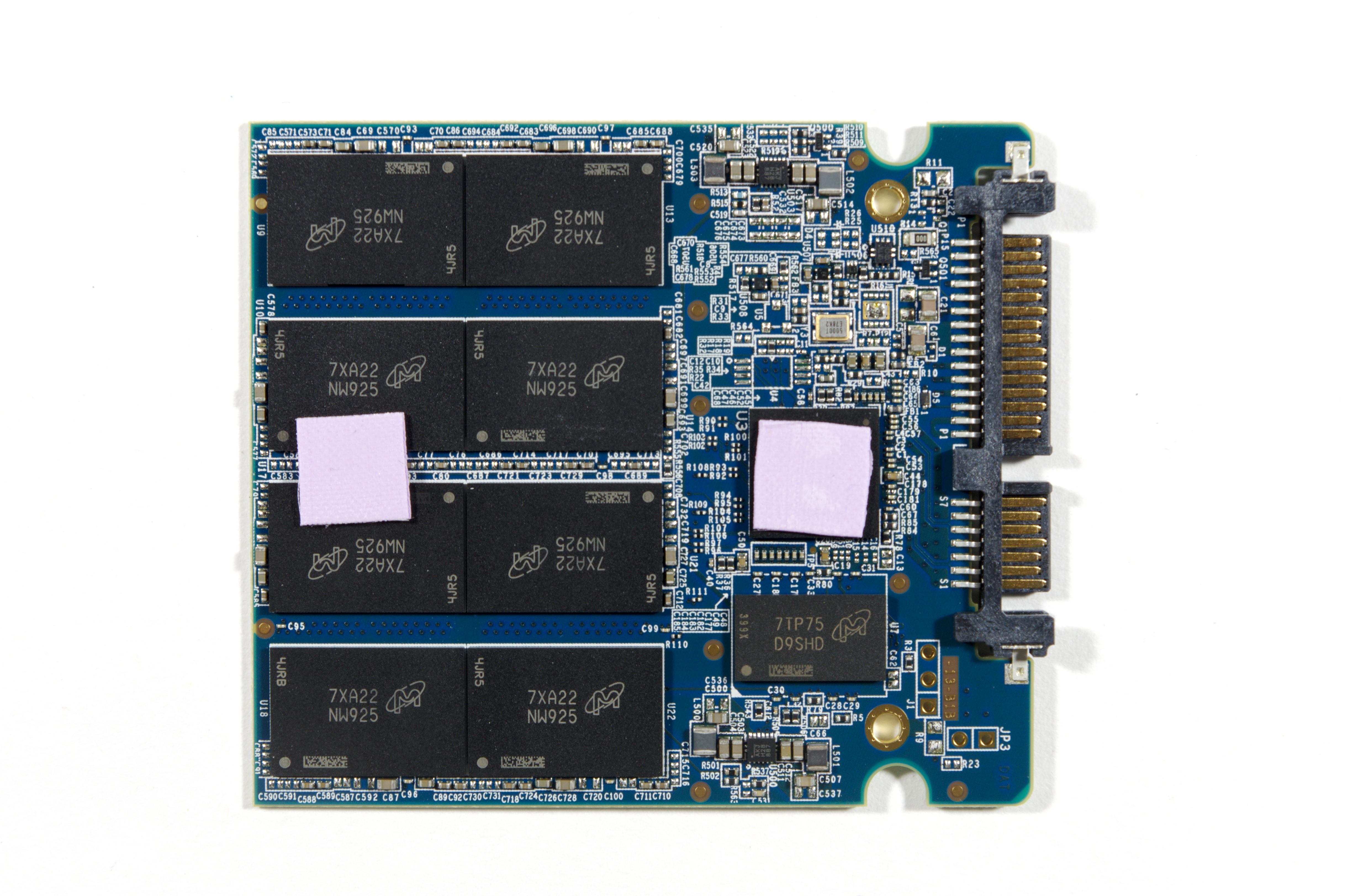
Internally, the 500GB MX500 uses the same PCB as the larger models. The back side is entirely blank, with the 8 NAND package locations and one DRAM spot unpopulated. On the front, we find the eight of the same dual-die NAND packages used on the 1TB model, plus 512MB of DRAM, the SM2258 controller, and all the usual smaller components.
| Crucial MX500 Specifications | |||||
| Capacity | 250 GB | 500 GB | 1 TB | 2 TB | |
| Form Factors | 2.5", M.2 2280 single-sided | 2.5", M.2 2280 single-sided | 2.5", M.2 2280 double-sided | 2.5" | |
| Controller | Silicon Motion SM2258 | ||||
| NAND | Micron 256Gb 64-layer 3D TLC | ||||
| Sequential Read | 560 MB/s | ||||
| Sequential Write | 510 MB/s | ||||
| 4KB Random Read | 95k IOPS | ||||
| 4KB Random Write | 90k IOPS | ||||
| Dynamic Write Acceleration (SLC Caching) | Yes, dynamically sized | ||||
| DevSleep Power | 2 mW | 2 mW | 4 mW | 25 mW | |
| Slumber Power | 55 mW | 55 mW | 65 mW | 110 mW | |
| Max Power | 3.0 W | 4.0 W | 5.0 W | 6.0 W | |
| Encryption | TCG Opal 2.0 & IEEE-1667 (eDrive) | ||||
| Endurance | 100 TB | 180 TB | 360 TB | 700 TB | |
| Warranty | Five years | ||||
| MSRP | $79.99 | $139.99 | $259.99 | $499.99 | |
With capacities from 250GB to 2TB now available at MSRPs that are highly competitive, the Crucial MX500 is shaking up the SATA SSD market. Last year's budget SSDs need big price cuts, and even mainstream drives like the SanDisk Ultra 3D are having to drop in price. M.2 versions of the Crucial MX500 up to 1TB are also on the way, so ultrabook users will have most of the same upgrade options.
For this review, we are focusing on the 500GB Crucial MX500. This is a lower capacity than we initially tested, making it more affordable and a bit slower than the 1TB model. With a MSRP of $139.99 and current retail prices slightly lower, the 500GB Crucial MX500 should prove to be a very popular product. Testing at the 500GB capacity point gives us the opportunity to make more direct comparisons against some other drives in our collection, especially the Intel 545s and the Crucial BX300.
| AnandTech 2017 SSD Testbed | |
| CPU | Intel Xeon E3 1240 v5 |
| Motherboard | ASRock Fatal1ty E3V5 Performance Gaming/OC |
| Chipset | Intel C232 |
| Memory | 4x 8GB G.SKILL Ripjaws DDR4-2400 CL15 |
| Graphics | AMD Radeon HD 5450, 1920x1200@60Hz |
| Software | Windows 10 x64, version 1709 |
| Linux kernel version 4.14, fio version 3.1 | |
- Thanks to Intel for the Xeon E3 1240 v5 CPU
- Thanks to ASRock for the E3V5 Performance Gaming/OC
- Thanks to G.SKILL for the Ripjaws DDR4-2400 RAM
- Thanks to Corsair for the RM750 power supply, Carbide 200R case, and Hydro H60 CPU cooler
- Thanks to Quarch for the XLC Programmable Power Module and accessories
Our SSD testbed's software has been updated for 2018 with a fresh Windows installation that corrects some problems with The Destroyer that cropped up during testing of the 1TB MX500. The testbed is now running Windows 10 version 1709 for the ATSB tests instead of version 1703. So far, the benchmark results on 1709 appear comparable to those from 1703, so this review uses a mix of old and new results. It is likely that results for NVMe drives will not be as closely comparable between Windows versions due to the ongoing development of Microsoft's NVMe driver, so all NVMe drives will be re-tested before inclusion in new reviews (And all the SATA drives will be retested too over the next two months to take advantage of the higher resolution power measurements from our new Quarch XLC Programmable Power Module.) The Linux-based synthetic benchmarks in this review are all fresh results with an updated 4.14 kernel and fio version 3, which brings much higher resolution timing measurements.
Both operating systems on this testbed have not been patched for the Meltdown or Spectre vulnerabilities, and the motherboard firmware has not been updated to include new CPU microcode. Testing is underway on other machines to determine the performance impact of the mitigation strategies. The primary testbed will remain in its current software and hardware configuration for now as the OS and microcode programmers continue to work toward stable and complete fixes.


25 Comments
View All Comments
PeachNCream - Friday, February 2, 2018 - link
"..the per-die capacity of the MX500's 64-layer 3D TLC is actually lower than that of the 32L 3D TLC.."Why is that the case? Shouldn't doubling the number of layers lead to greater capacity and does this mean that there are more ICs per GB in the newer MX500? I'm super confused.
jtd871 - Friday, February 2, 2018 - link
"The Crucial MX500 uses Micron's 256Gb 64L 3D TLC part and consequently returns to the standard drive capacities and overprovisioning ratios, instead of the unusual configurations caused by the 384Gb die capacity in the MX300's 32L 3D TLC. The slightly lower usable capacities of the MX500 than the MX300 means the new drives have slightly higher prices on a per-GB basis, but the MSRPs are still very competitive against current street prices for the competition."So the new chips have more layers per package, but less overall capacity. I'll guess the 384Gb die hamstrung performance on relatively smaller-capacity drives by offering fewer memory channels for the processor to work with simultaneously. Plus, I'll guess that it was a bit of an oddball size for the algorithms to deal with.
FunBunny2 - Friday, February 2, 2018 - link
large node?more area dedicated to control functions?
Billy Tallis - Friday, February 2, 2018 - link
For the 32L node, IMFT was more or less prioritizing MLC use cases by making a 256Gb MLC die that could be used as a 384Gb TLC part. For the 64L node, TLC is the priority and they're making both 256Gb TLC and 512Gb TLC parts. The latter should be cheaper per GB when it is available, but would be a worse choice for small consumer drives. The 256Gb die is really tiny, which makes it more appealing to the mobile market than a lot of previous IMFT parts.FunBunny2 - Saturday, February 3, 2018 - link
"making a 256Gb MLC die that could be used as a 384Gb TLC part."so... does this mean that NAND is all the same, and it's the controller that decides among S/M/T?? or is it the case that S can be coerced to M, and M to T, but not the other way round? is there a tute, here or elsewhere, that tells us the nittygritty about why titular NAND can/can't be used at other densities?
FunBunny2 - Saturday, February 3, 2018 - link
well, I did find one, but from 2012 (and AT: https://www.anandtech.com/show/5067/understanding-... )"This array can be turned into either SLC, MLC, or TLC. The actual array and transistors are equivalent in all three flash types; there is no physical difference. "
some/many folks have been claiming that TLC, in particular, is physically different from SLC. is that now true?
Kristian Vättö - Sunday, February 4, 2018 - link
In terms of memory cell design, SLC, MLC and TLC can be the same, but the peripheral circuit design isn't (min # of latches = # of bits per cell). More bits per cell designs are also likely to have more spare/ECC bytes per page.In layman terms, TLC and MLC can be run as pseudo-SLC by only programming the lower page, but it's impossible to run e.g. MLC as TLC. But pseudo-SLC isn't the same thing as native SLC.
Spatty - Wednesday, February 14, 2018 - link
SLC/MLC chips are physically the same chips during the fab process. Maybe some Implant changes but die layout is the same. In Probe, circuits are blown to make them SLC or MLC.The referenced quote in this thread, is that a due to the usage of die vs chip/package. The chips in the images can have multiple die in one single chip/package and thus the 'density' of the chip/package changes. More layers still means more bits/mm^2.
PeachNCream - Monday, February 5, 2018 - link
Thanks Billy! It makes more sense now.colonelclaw - Friday, February 2, 2018 - link
I'm wondering, would it be worth adding a PS4 Pro/'BoneX benchmark to SATA SSD reviews? The 1TB is fast becoming a worthwhile, if luxurious, upgrade for the top consoles. It may be slightly unaffordable now, but possibly not for long?