TSMC Teams Up with ARM and Cadence to Build 7nm Data Center Test Chips in Q1 2018
by Anton Shilov on September 14, 2017 11:45 AM EST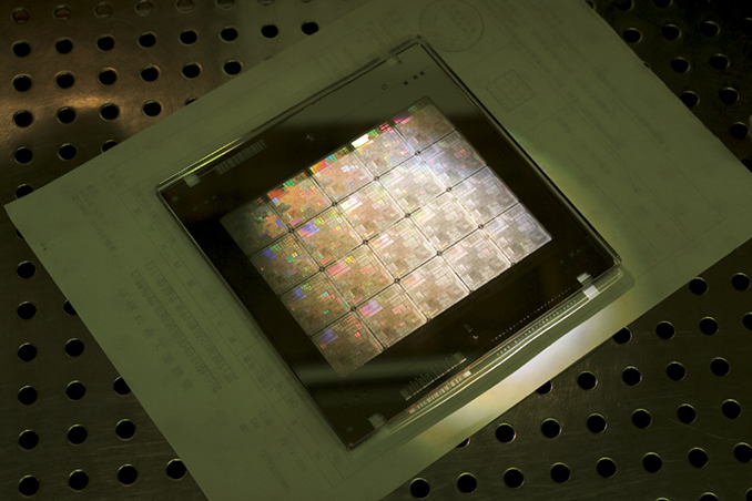
TSMC has announced plans to build its first test chips for data center applications using its 7 nm fabrication technology. The chip will use compute cores from ARM, a Cache Coherent Interconnect for Accelerators (CCIX), and IP from Cadence (a DDR4 memory controller, PCIe 3.0/4.0 links). Given the presence of the CCIX bus and PCIe 4.0 interconnects, the chip will be used to show the benefits of TSMC’s 7 nm process primarily for high-performance compute (HPC) applications. The IC will be taped out in early Q1 2018.
The 7 nm test chips from TSMC will be built mainly to demonstrate capabilities of the semiconductor manufacturing technology for performance-demanding applications and find out more about peculiarities of the process in general. The chip will be based on ARMv8.2 compute cores featuring DynamIQ, as well as a CMN-600 interconnect bus for heterogeneous multi-core CPUs. ARM and TSMC do not disclose which cores they are going to use for the device - the Cortex A55 and A75 are natural suspects, but that’s a speculation at this point. The new chip will also have a DDR4 memory controller as well as PCI Express 3.0/4.0 links, CCIX bus and peripheral IP buses developed by Cadence. The CCIX bus will be used to connect the chip to Xilinx’s Virtex UltraScale+ FPGAs (made using a 16 nm manufacturing technology), so in addition to implementation of its cores using TSMC’s 7 nm fabrication process, ARM will also be able to test Cadence’s physical implementation of the CCIX bus for accelerators, which is important for future data center products.
| TSMC's 7 nm Test Chip at Glance | ||||
| Logic | PHY | |||
| Compute Cores | ARM v8.2 with DynamIQ | |||
| Internal Interconnect Bus | ARM CMN-600 | |||
| CCIX | Cadence | |||
| DDR4 DRAM Controller | ? | Cadence | ||
| PCI Express 3.0/4.0 | Cadence | |||
| Peripheral Buses | I2C, SPI and QSPI by Cadence | |||
| Verification and Implementation Tools | Cadence | |||
As reported multiple times, TSMC’s 7 nm manufacturing process will be a “long” node and the foundry expects the majority of its large customers to use it. By contrast, the current 10 nm technology is aimed primarily at developers of smartphone SoCs. TSMC projects that its first-generation CLN 7FF fabrication technology, compared to its CLN16FF+, will enable its customers to reduce power consumption of their chip by 60% (at the same frequency and complexity), increase their clock rate by 30% (at the same power and transistor count) and shrink their die sizes by 70% at the same complexity. Sometime in 2019, TSMC plans to start making chips using its CLN7FF+ process technology with EUV for critical layers. TSMC claims that the CLN7FF+ will enable the company’s customers to further increase transistor density while improving other areas, such as yields and power consumption.
TSMC does not disclose which of its 7 nm process technologies announced so far it is going to use for the test chip, but the use of EUV for test chips is something that cannot be excluded. For example, GlobalFoundries claims that they use EUV to accelerate production of test chips. On the other hand, since design rules for CLN7FF and CLN7FF+ are different, it is highly likely that TSMC conservatively uses the former for the test chip.
TSMC’s CLN7FF process tech passed qualification in April and was expected to enter risk production in Q2 2017, according to TSMC’s management. The foundry expected 13 CLN7FF tape outs this year and it is projected that the fabrication technology would be used commercially starting from Q2 2018. Therefore, taping out the test vehicle using the first-gen DUV-only 7 nm process in Q1 2018 seems a bit late for early adopters who intend to ship their 7 nm SoCs in the second half of next year. Meanwhile, early adopters (read: Apple, Qualcomm, and some others) get access to new process technologies long before their development is completed and final PDKs (process development kits) are ready. Keeping in mind that the test chips feature a CCIX and PCIe 4.0 buses, it is clearly designed to show advantages of TSMC’s 7 nm process technologies for HPC applications. In fact, this is what TSMC says itself:
“Artificial intelligence and deep learning will significantly impact industries including media, consumer electronics and healthcare,” said Dr. Cliff Hou, TSMC vice president, Research & Development/Design and Technology Platform. “TSMC’s most advanced 7nm FinFET process technology provides high performance and low power benefits that satisfy distinct product requirements for High-Performance Computing (HPC) applications targeting these markets.”
Related Reading
- GlobalFoundries Details 7 nm Plans: Three Generations, 700 mm², HVM in 2018
- Intel to Equip Fab 42 for 7 nm
- Samsung and TSMC Roadmaps: 8 and 6 nm Added, Looking at 22ULP and 12FFC
- ARM Launches DynamIQ: big.Little to Eight Cores Per Cluster
- ARM Announces Mali-G72: Bifrost Refined for the High-End SoC
- ARM Announces Mali-G72: Bifrost Refined for the High-End SoC
Source: TSMC


11 Comments
View All Comments
wiineeth - Thursday, September 14, 2017 - link
Is Nvidia volta going to be based on 7nm?edzieba - Thursday, September 14, 2017 - link
GV100 is on 12nm FFN, so smaller Volta dies are likely to use the same process.tipoo - Thursday, September 14, 2017 - link
And 12nm is an extension of their 16nm fwiw. In intel terms it would probably be the ++ node.Qwertilot - Thursday, September 14, 2017 - link
Not likely - V100 isn't. Son of Volta presumably will.tipoo - Thursday, September 14, 2017 - link
If 14nm is actually a 20nm back end, what exactly does "7nm" mean?HStewart - Thursday, September 14, 2017 - link
Using what you just wrote ( 20/14 * 7 ) = 10But there is stories that the size from different makes don't always equal the same on another makers process.
I not an chip technical manufacturer ( even though I did take some classes in micro code in college ) - but maybe a better indication of process is taking the density of transistors per square area.
FreckledTrout - Thursday, September 14, 2017 - link
Agree HStewart, density would be a better measure as the nm feature size is mostly marketing since only some features are at that size and with these "3D" chips there is so much more to the resulting density that I would much rather they market it that way. At the end of the day they can call it whatever they want, the people paying to have chips made on this process will know exactly what kind of densities they will get even if none of us get to see that data.HStewart - Thursday, September 14, 2017 - link
Agreed - one example of this is AMD Threadripper vs Skylark Xhttp://digiworthy.com/2017/06/22/intel-skylake-x-v...
If you look at above link - the die size is pretty close - but it also appears that AMD has a lot of wasted space - not referring to Zen modules not in use. I don't know the exact transistor counts - but it looks like Intel has more transistors for each related size.
To AMD's merit, I would think it cost less to engine modules to fit together instead having more cores - it would be cheaper processed - to me it kind of like multi-cpu server box using single chip. So a dual cpu 32 core AMD Server chip is kind of like a 8 cpu 8 core MP system.
I believe Microsoft had to special changes to it operating systems so zen architecture does not count as multi-cpu setup.
MrSpadge - Thursday, September 14, 2017 - link
http://semiengineering.com/a-node-by-any-other-nam...So transistor gate length of 14 - 18 nm, depending on size and way of counting.
ImSpartacus - Friday, September 15, 2017 - link
The numbers mean nothing. It's all marketing.We live in a world where TSMC is upset because their "16" is higher than their competitor's "14", so they renamed it to "12" because "12" is less than "14".