Hot Chips 2016: Exynos M1 Architecture Disclosed
by Joshua Ho on August 25, 2016 8:00 AM EST- Posted in
- Mobile
- Samsung
- Hot Chips
- Exynos
- LSI
- Trade Shows
- Exynos 8890
- Exynos M1
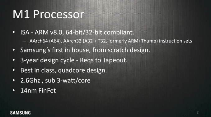
While we can always do black-box testing to try and get a handle for what a CPU core looks like, there’s really only so much you can do given limited time and resources. In order to better understand what an architecture really looks like a vendor disclosure is often going to be as good as it gets for publicly available information. The Exynos M1 CPU architecture is Samsung’s first step into a custom CPU architecture for an mobile SoC. Custom CPU architectures are hardly a trivial undertaking, so it’s unlikely that a company would make the investment solely for a marketing bullet point.
With that said, Samsung has provided some background for the Exynos M1, claiming that the design process started about 3 years ago in 2013 around the time of the launch of the Galaxy S4. Given the issues that we saw with Cortex A15 in the Exynos 5410, it's not entirely unsurprising that this could have been the catalyst for a custom CPU design. However, this is just idle speculation and I don't claim to have any knowledge of what actually led to Exynos M1.
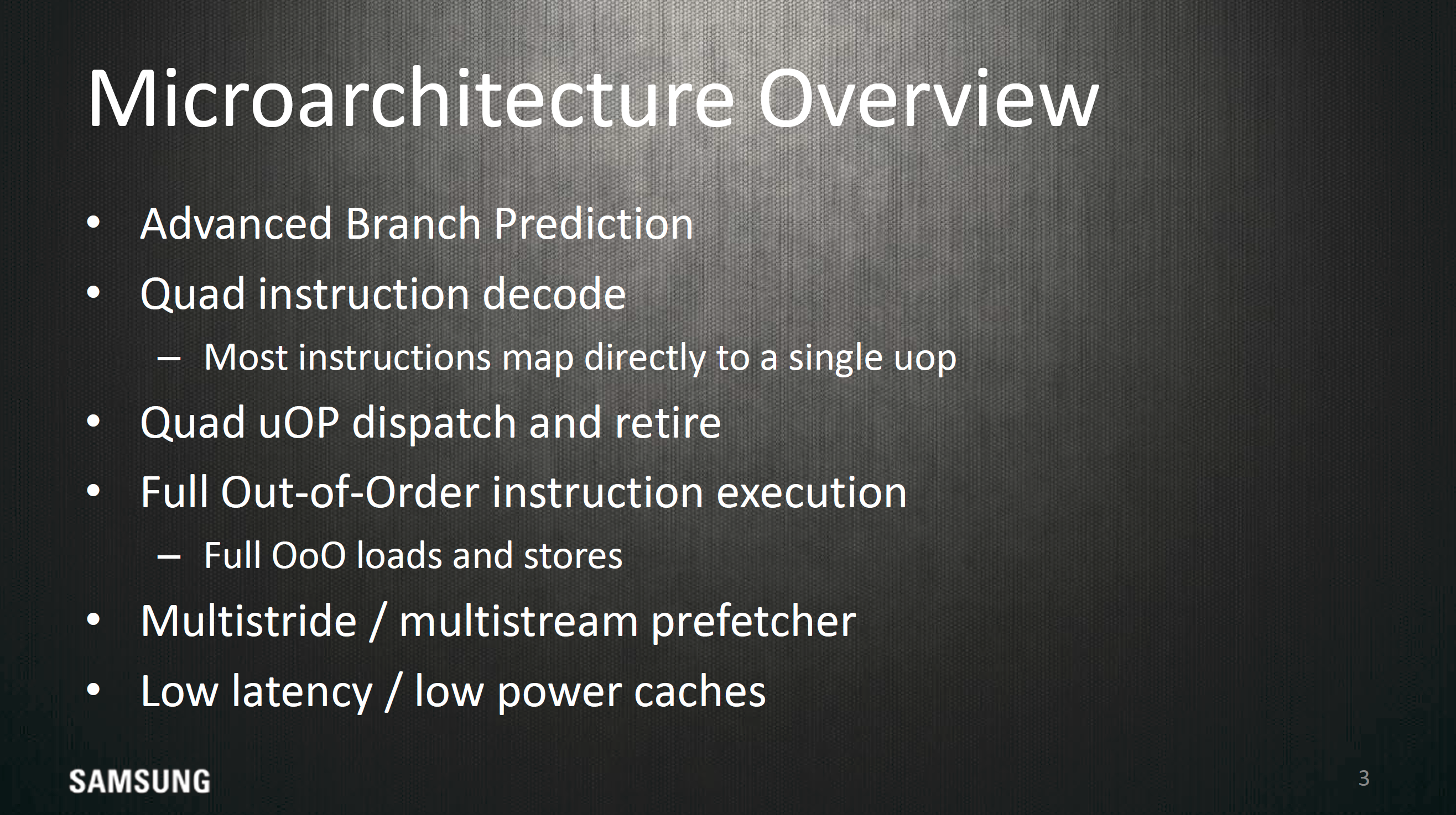
At a high level, Samsung pointed out that the Exynos M1 is differentiated from other ARM CPU designs by advanced branch prediction, roughly four instructions decoded per cycle, as well as the ability to dispatch and retire four instructions per cycle. As the big core in the Exynos 8890, it obviously is an out of order design, and there are some additional claims of multistride/stream prefetching and improved cache design.
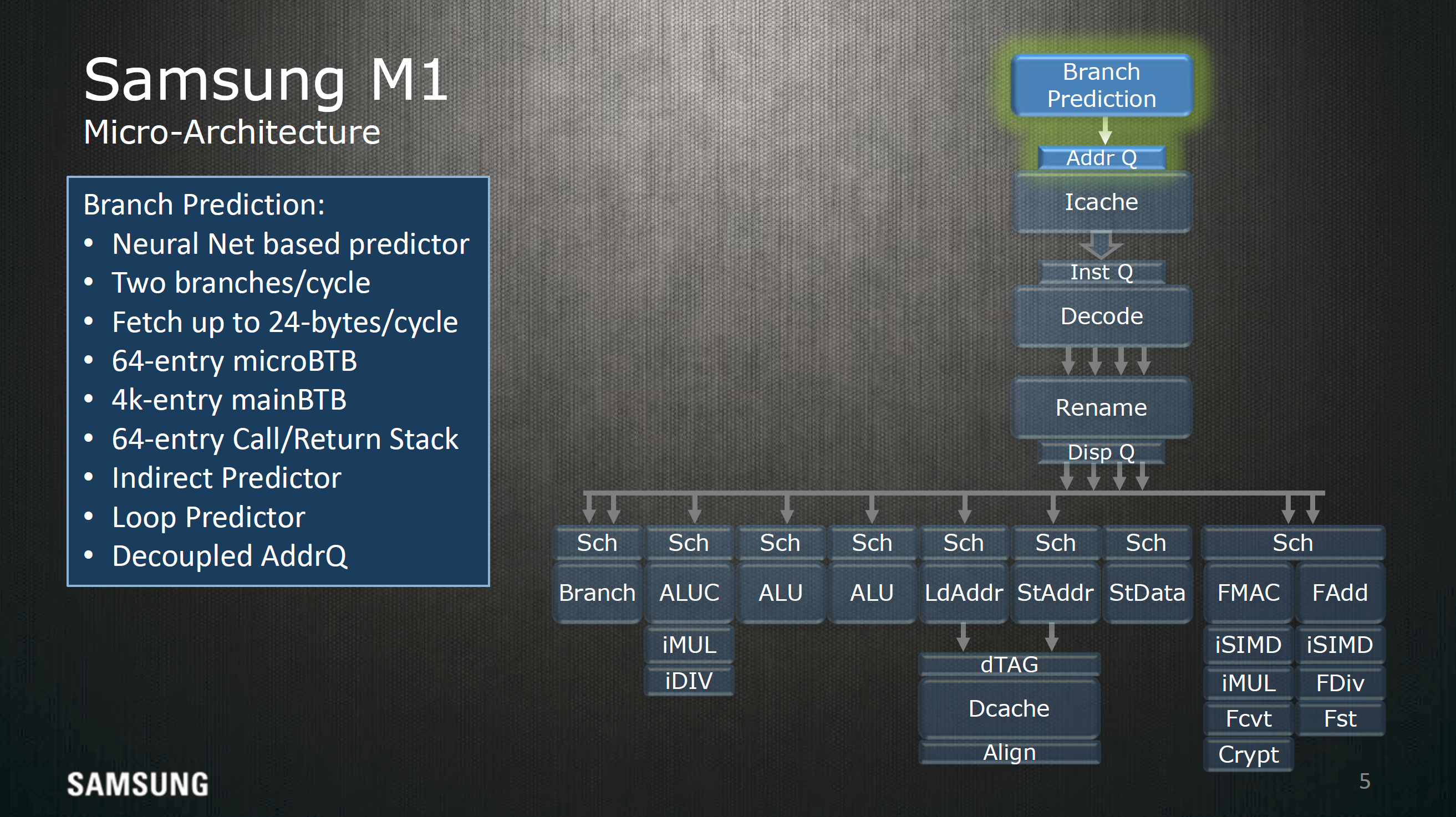
Starting with branch prediction, the major highlight point here is that the branch predictor uses a perceptron of sorts to reduce the rate at which branches miss. If you understand how pipelining works, it takes a significant amount of time to reload saved state and invalidate the execution that occurred after an incorrect branch. I’m no expert here but it looks like this branch predictor also has the ability to do multiple branch predictions at the same time, either as a sort of multi-level branch predictor or handling multiple successive branches. Perceptron branch prediction isn't exactly new in academia or in real-world CPUs, but it's interesting to see that this is specifically called out when most companies are reluctant to disclose such matters.
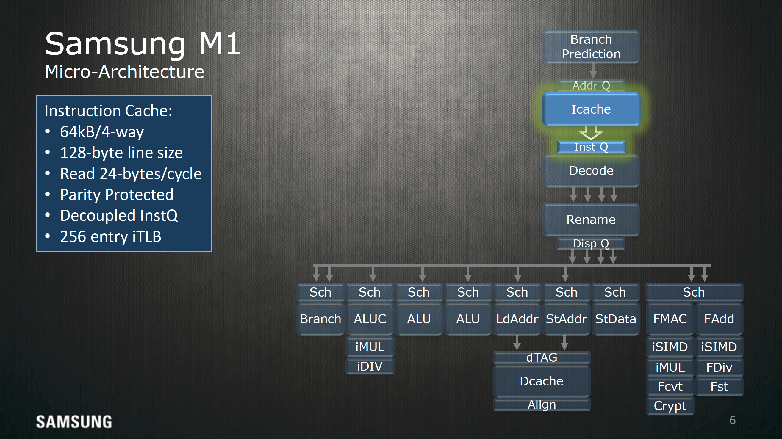
Moving past branch prediction we can see some elements of how the cache is set up for the L1 I$, namely 64 KB split into four sets with 128-byte line sizes for 128 cache lines per set, with a 256 entry TLB dedicated to faster virtual address translation for instructions. The cache can read out 24 bytes per cycle or 6 instructions if the program isn’t using Thumb instruction encoding.
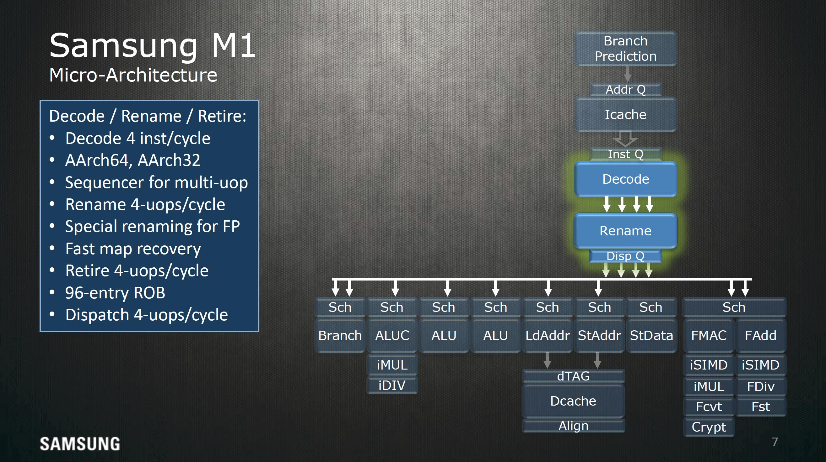
On the instruction side we find decode, rename, and retire stages, register rename logic. The decode stage can handle up to 4 instructions per clock while the retire, and dispatch systems are all capable of handling four instructions every cycle, so best case throughput is going to be four instructions per cycle assuming the best-case scenario that the ARM instruction is a single micro-operation.
Other areas of interest include the disclosure of a 96 entry reorder buffer, which defines how many instructions can be in-flight at any given time. Generally speaking more entries is better for extracting ILP here, but it’s important to understand that there are some significant levels of diminishing returns in going deeper, so doubling the reorder buffer doesn’t really mean that you’re going to get double the performance or anything like that. With that said, Cyclone’s reorder buffer size is 192 entries and the Cortex A72 has 128 entries, so the size of this buffer is not really anything special and is likely a bit smaller in order to cut down on power consumption.
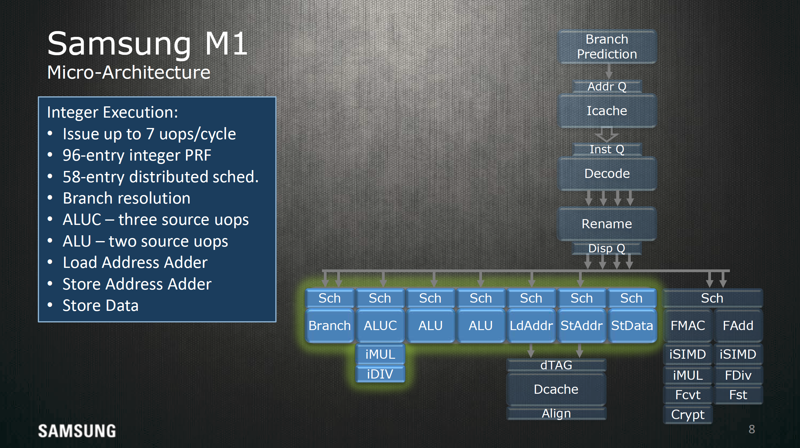
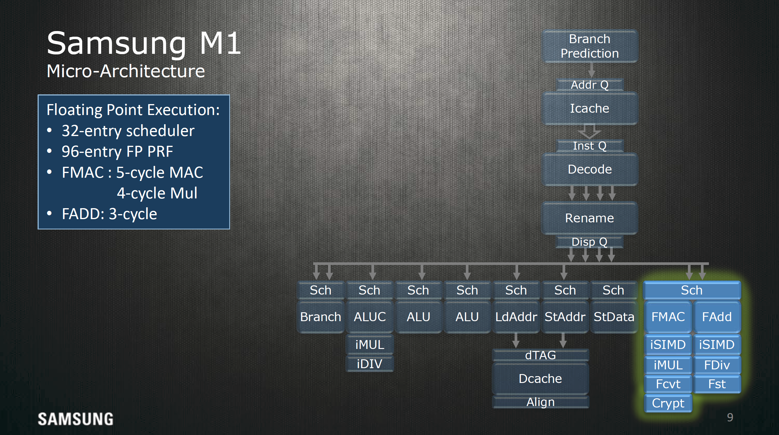
For integer execution the Exynos M1 has seven execution ports, with most execution pipelines getting their own dedicated schedulers. It's to be noted that the branch monitor is able to be fed 2 µops per cycle. On the floating point side it looks like almost everything shares a single 32 entry scheduler, which can do a floating point multiply-accumulate operation every 5 cycles and a floating point multiplication every 4 cycles. Floating point addition is a 3 cycle operation.
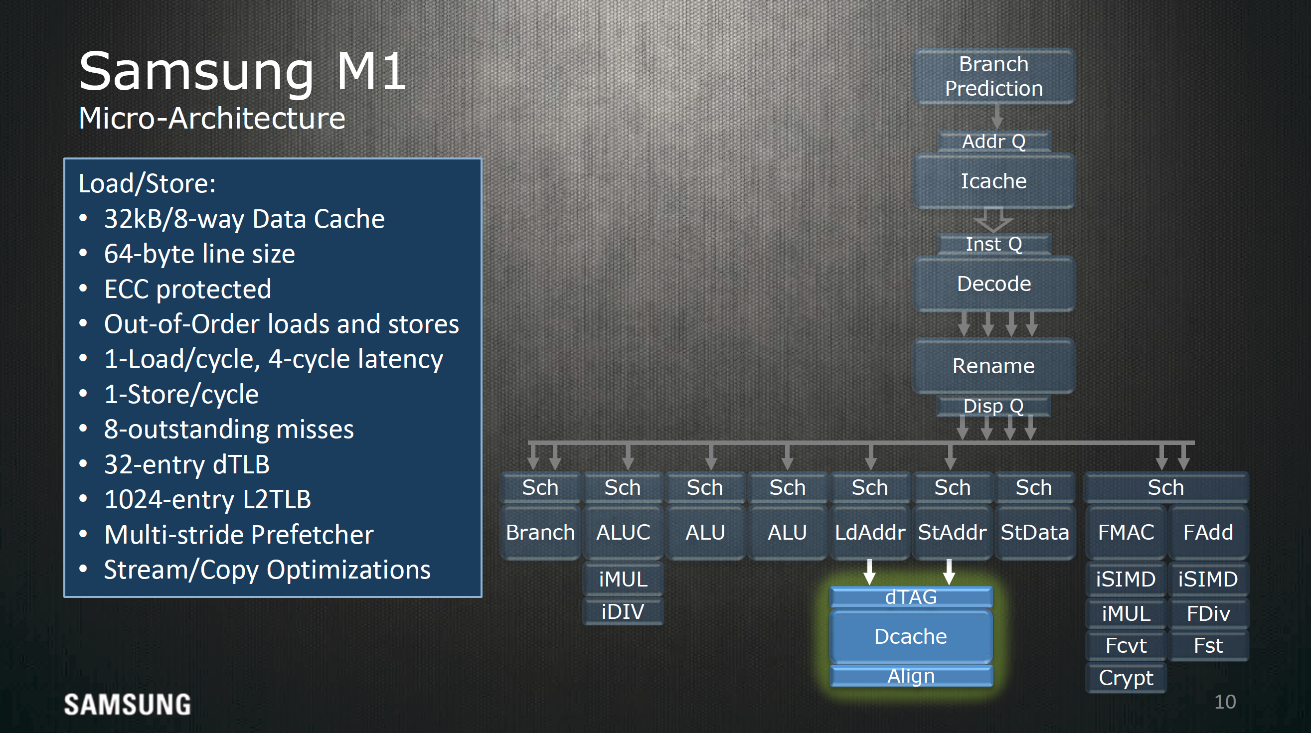
For loads and stores, a 32 KB, 8-way set associative cache with 64 byte line size is used as well as a 32 entry dTLB and 1024 entry L2 dTLB to hold address translations and the associated data for any given address, and allows out of order loads and stores to reduce visible memory latency. Up to 8 outstanding cache misses for loads can be held at any given time, which reduces the likelihood of stalling, and there are additional optimizations for prefetching as well as optimizations for other types of memory traffic.
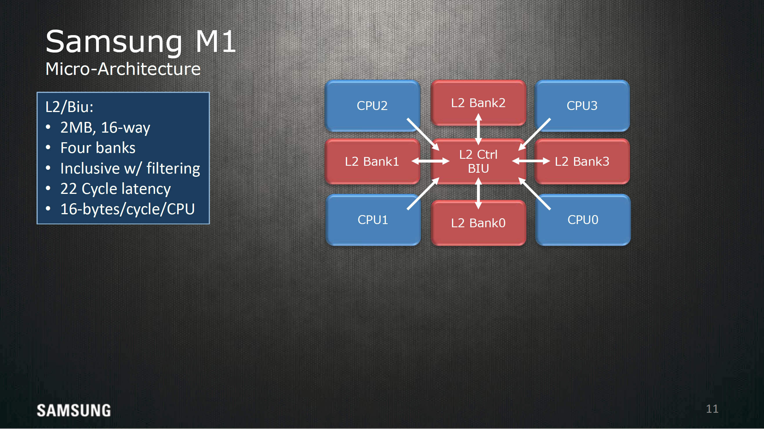
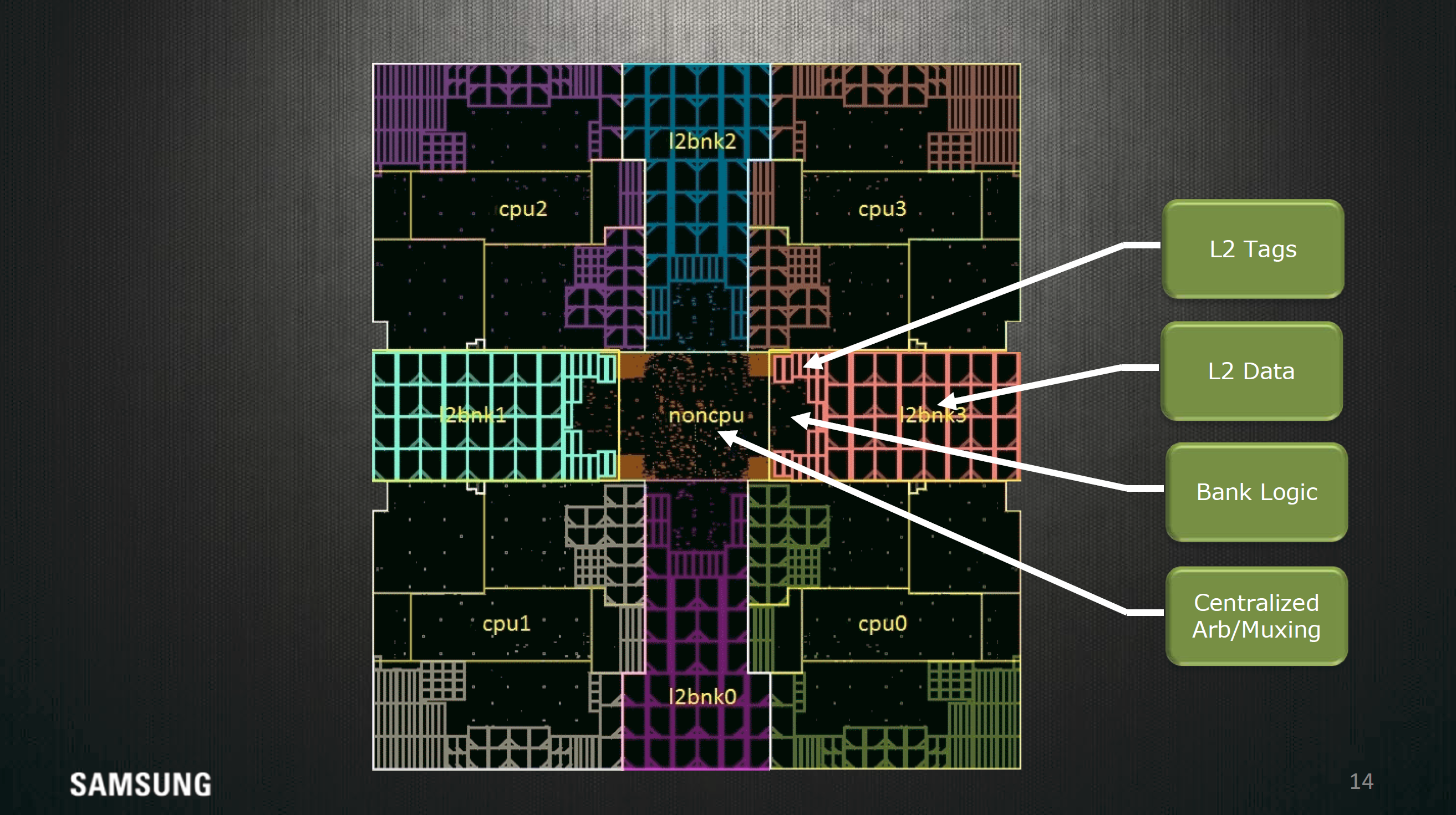
The L2 cache here is 2MB shared across all cores split into 16 sets. This memory is also split into 4 banks and has a 22 cycle latency and has enough throughput to fill two AArch64 registers every cycle, and if you look at the actual floorplan this diagram is fairly indicative of how it actually looks on the die.
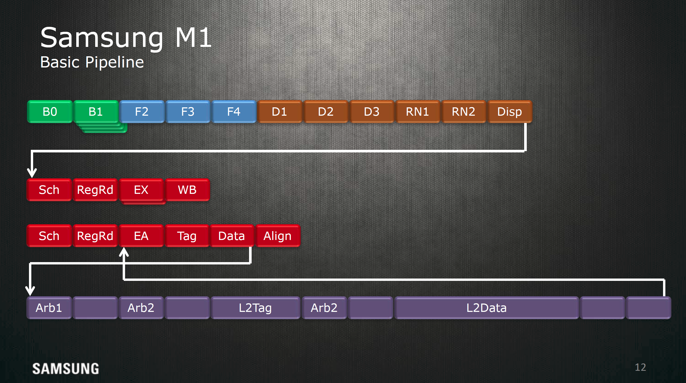
Samsung also highlighted the pipeline of the Exynos M1 CPU at a high level. If you're familiar with how CPUs work you'll be able to see how the basic stages of instruction fetch, decode, execution, memory read/write, and writeback are all present here. Of course, due to the out of order nature of this CPU there are also register rename, dispatch, and scheduling stages.
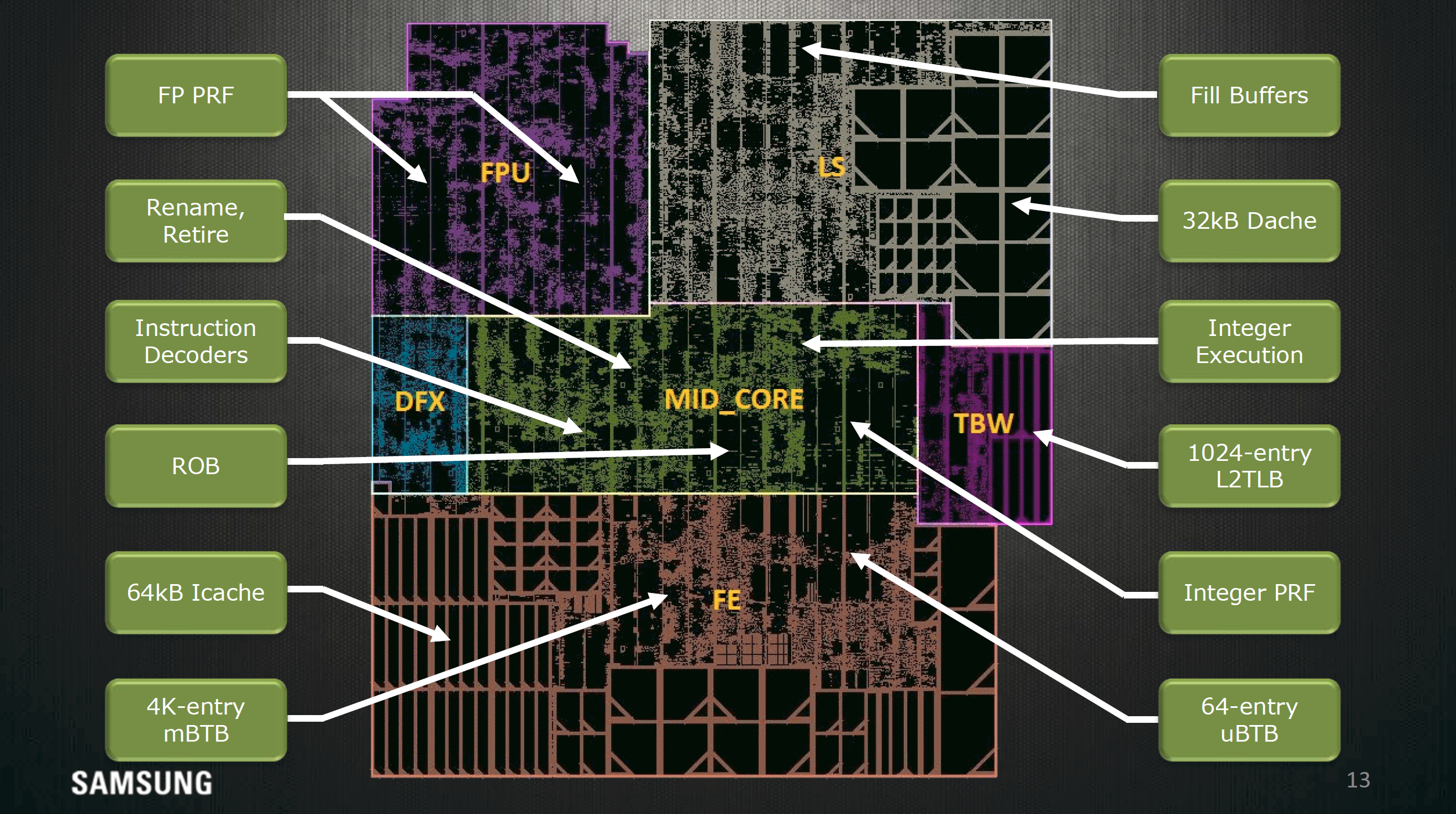
It's fairly rare to see this kind of in-depth floorplanning shots from the designers themselves, so this slide alone is interesting to see. I don't have a ton to comment on here but it's interesting to see the distances of all the components of the CPU from the center of the core where most of the execution is happening.
Overall, for Systems LSI's first mobile CPU architecture it's impressive just how quickly they turned out a solid design in three years from inception to execution. It'll be interesting to see what they do next once this design division really starts to hit its stride. CPU architectures are pipelined to some extent, so even if it takes three years to design one, if the mobile space as a whole is anything to go by then it's likely that we'll be seeing new implementations and designs from this group in the next year or two. Given the improvements we've seen from the Exynos 5420 to 7420 it isn't entirely out of question that we could see much more aggressive execution here in the near future, but without a crystal ball it's hard to say until it happens.


29 Comments
View All Comments
Eden-K121D - Thursday, August 25, 2016 - link
So when are we getting a deepdive on SD 820 and Exynos 8890hans_ober - Thursday, August 25, 2016 - link
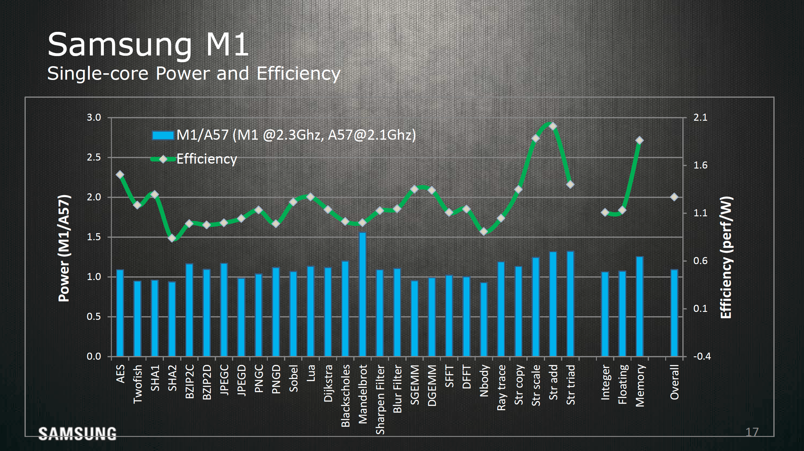
The power analysis with the Intel x86 SoC, Tegra 3 and Snapdragon from some years back needs to be repeated..ddriver - Thursday, August 25, 2016 - link
Sure, because it must be rehashed "how superior" atom is to arm, which would explain intel's domination complete and utter domination of the mobile device market.... oh what, that's right, that's not a thing.Wonder about the gaps in the last chart, did they censor some stuff too good to know about?
On a side note, while performance is meh, efficiency seems pretty good, they should make a 16 core version of it!
frenchy_2001 - Thursday, August 25, 2016 - link
The gaps are obviously for legibility, as they are between individual tests, type and overall.They seem to be a bit more powerful than A57 (about 10%) overall, while being about 25% more efficient. Would be nice to compare with A72, as A57 was rather power hungry.
Ariknowsbest - Friday, August 26, 2016 - link
After two weeks with my new phone the A72 (Kirin 950) seems very efficient, compared to the S808 (work phone) or S801 (own). Wasn't impressed by the A57 so I stayed longer with 32-bit on Android.Gasaraki88 - Wednesday, August 31, 2016 - link
A lot of products are superior to others yet don't do well in the markets due to various reasons. Just because Atom is dead doesn't mean is wasn't a good chip. (Beta vs. VHS, etc)RaduR - Thursday, August 25, 2016 - link
If they could only start using PowerVR instead of Mali then we could have a real competition to Qualcomm SD. Unfortunately even midrange SD 650 is has faster Graphics than Mali.CPU is not enough they need strong GPU and PowerVR looks like the only viable option to compete with QComm
ZenX - Thursday, August 25, 2016 - link
Exynos 8890 could've matched SD820 in graphics if they used the top of the line Mali T880-MP16, but instead Samsung decided to shelve 4 cores and end up with MP12 insteadmczak - Thursday, August 25, 2016 - link
The Mali T880-MP12 in the Exynos 8890 already has to throttle like crazy in any kind of sustained load (about half the peak performance). It is true generally wider but lower clocked designs are more power efficient, but compared to other chips using Mali T8xx graphic the max graphic clock is already pretty low, so it seems unlikely efficiency would be better with lower clocks. Thus, all a MP16 version would achieve would be higher (useless) peak performance.IMHO Samsung could have just used a MP8 version instead with very little loss of actual real world performance (but the same is true for the Adreno 530 too, a somewhat smaller configuration would achieve the same practical performance by not needing to throttle that much).
lilmoe - Thursday, August 25, 2016 - link
Stop looking too much into benchmarks. Mali has been faster and more efficient for a while in real world usage.