Analyzing Intel’s Discrete Xe-HPC Graphics Disclosure: Ponte Vecchio, Rambo Cache, and Gelato
by Dr. Ian Cutress on December 24, 2019 9:30 AM ESTThe First Xe-HPC Deployment: Aurora, with Xe Link
Some of this analysis is taken from our original Aurora Xe news post, but now with Xe Link information.
If you’ve skipped to this final page, it’s worth reading the last few. We’ve covered in detail what we can derive from Intel slides about the Xe architecture, the new Xe-HPC hardware paradigm, the Ponte Vecchio GPU in as much detail as we could figure out, and the new software strategy. All this page talks about is the major commercial deployment of Xe-HPC in a supercomputer: Aurora. If you want the juicy details on the hardware, and what we might see on the graphics side, take a read of the previous pages.
Aurora: Exascale in the USA
Part of the announcement at HPC DevCon was about the first deployment of Ponte Vecchio, to the new Aurora supercomputer for the Department of Energy at Argonne National Laboratories. Intel disclosed that it will be delivering Aurora in 2021, featuring two new future CPUs as well as six GPUs per node.
Intel has been working on the Aurora contract for a while now, and the project has changed scope over time due to market changes and hardware setbacks. Initially announced several years ago as a ‘deliver by 2020’ project between Argonne, Cray, and Intel, the hardware was set to be built around Intel’s Xeon Phi platform, providing high-throughput acceleration though Intel's AVX-512 instructions and the 10nm Knights Hill accelerator. This announcement was made before the recent revolution in AI acceleration, as well as Intel subsequently killing off the Xeon Phi platform after adding AVX-512 to its server processors (with the last breath Knights Mill receiving a very brief lifespan). Intel had to go back to the drawing board, and since Xeon Phi was scrapped, Intel’s audience has been questioning what it will bring to Aurora, and until today the company had only said that it would be built from a combination of Xeon CPUs and XeHPC GPUs.
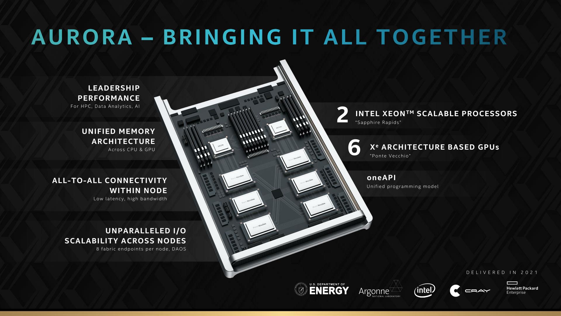
The two CPUs will be ‘Sapphire Rapids’ Xeon CPUs, which if you follow Intel’s release schedule, is the CPU after the CPU after the CPU after the one currently on the market. It goes Skylake, Cascade Lake (currently out), Cooper Lake (2019/2020), Ice Lake (2H2020), Sapphire Rapids (2021). The promise is that these CPUs will be on 10nm, and judging by the diagram will have 8 channels of memory (likely DDR5, but not confirmed). Sapphire Rapids are predicted to be Intel’s first enterprise CPUs to support the new CXL standard, which would also mean PCIe 5.0 support at a minimum.
With the two CPUs are six Ponte Vecchio GPUs. Judging by the diagram, it must be pretty obvious that these are not PCIe cards, but likely to be OAM or SXM2 modules, or whatever the newest standard will be at the time. Each GPU will be able to communicate directly to each other via CXL, which is an interesting element to the discussion. On these diagrams is a small black chip in the middle, which Intel announced as its new Xe Link chip.
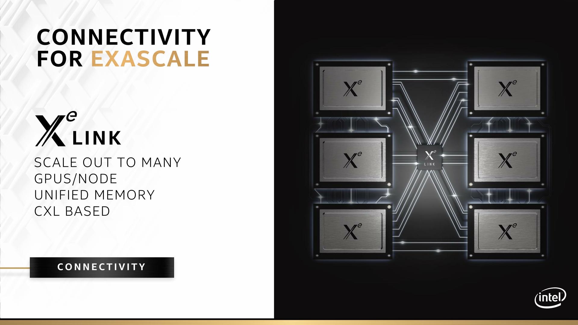
Much like NVIDIA’s NVSwitch, it looks like the Xe Link chip is there to mediate communications between all the GPUs in a node, and by what Intel says on this slide, between nodes as well. It would appear to also manage the unified memory of the system, and like the GPUs, it is CXL based. Part of the announcement on the links between the GPUs is that it should be an all-to-all design, despite the image above showing some GPUs communicating directly to each other and some only through the Link chip. We confirmed that this representation was inaccurate.
The CPUs will be Sapphire Rapids CPUs, Intel’s second generation of 10nm server processors coming after the Ice Lake Xeons. The announcement today reaffirmed that Sapphire Rapids is a 2021 processor; and likely a late 2021 processor, as the company also confirmed that Ice Lake will have its volume ramp through late 2020. Judging from Intel's images, Sapphire Rapids is set to have eight memory channels per processor, with enough I/O to connect to three GPUs. Within an Aurora node, two of these Sapphire Rapids CPUs will be paired together, and support the next generation of Intel Optane DC Persistent Memory (2nd Gen Optane DCPMM). We already know from other sources that Sapphire Rapids is likely to be DDR5 as well, although I don't believe Intel has said that outright at this point.
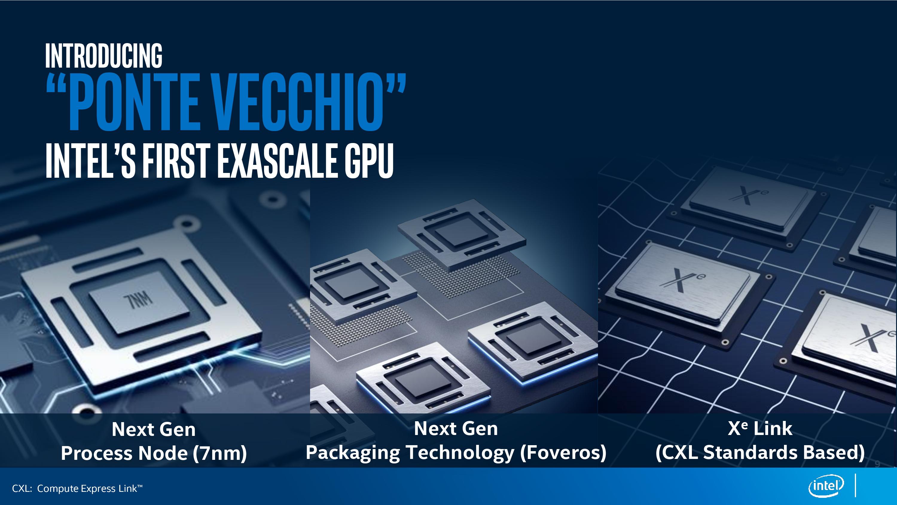
On the GPU side, all six of the GPUs per node will be Intel’s new 7nm Ponte Vecchio Xe GPU.
Each Aurora node will have 8 fabric endpoints, giving plenty of topology connectivity options. And with the system being built in part by Cray, connecting the systems will be a version of their Slingshot networking architecture, which is also being used for the other early-2020s US supercomputers. Intel has stated that Slingshot will connect ~200 racks for Aurora, featuring a total of 10 petabytes of Memory and 230 petabytes of Storage.
Guessing Ponte Vecchio Performance
With this information, if we spitball some numbers on performance, here's what we end up with:
- Going with Intel's number of 200 racks
- Assume each rack is a standard 42U,
- Each Aurora node is a standard 2U,
- We know the system has 200 racks.
- Take out 6U per rack for networking and support,
- Take out 1/3 of the racks for storage and other systems
- We get a rounded value of 2400 total Aurora nodes (2394 based on assumptions).
This means we get just south of 5000 Sapphire Rapids CPUs and 15000 Ponte Vecchio GPUs for the whole of Aurora. Now when calculating the total performance of a supercomputer, the CPU and Accelerator performance often depends on the workload required. If Ponte Vecchio is truly an exascale class GPU, then let’s assume that the GPUs are where the compute is. If we divide 1 ExaFLOPs by 15000 units, we’re looking at 66.6 TeraFLOPs per GPU. Current GPUs will do in the region of 14 TF on FP32, so we could assume that Intel is looking at a ~5x increase in per-GPU performance by 2021/2022 for HPC. Of course, this says nothing about power consumption, and if we were to do the same math at 4U per node, then it would be ~7500 GPUs, and we would need 135 TF per GPU to reach exascale.
Delivering The Hardware
Despite initially being a ‘deliver by 2020’ project, Intel is now saying that Aurora will be delivered in 2021. This means that Intel has to execute on the following:
- Manufacturing at 10++ in sufficient yield with respect to cores/frequencies
- Manufacturing at 7nm for chiplets, both in yield and frequencies
- Transition through DDR3 to DDR4 (and DDR5?) in that time frame
- Transition through PCIe 3.0 to PCIe 4.0 and PCIe 5.0 in that time frame
- Release and detail its 2nd generation Optane DC Persistent Memory
- Provide an SDK to deal with all of the above
- Teach researchers to use it
On those last two points, Intel has stated that Ponte Vecchio and Aurora will be a primary beneficiary of the company’s new OneAPI SDK. This industry initiative, spearheaded by Intel, is designed to use a singular cross-architecture language called ‘Data Parallel C++’, based on C++ and SYCL, that can pull libraries designed to speak to various elements of Intel’s hardware chain. The idea is that software designs can write the code once, link appropriate libraries, and then cross-compile for different Intel hardware targets. In Intel’s parlance, this is the ‘xPU’ strategy, covering CPU, GPU, FPGA, and other accelerators. Aside from Argonne/Cray, Intel is citing Lenovo and Atos as key partners in the OneAPI strategy.

In order to achieve a single exascale machine, you need several things. First is hardware – the higher performance a single unit of hardware, the fewer you need and the less infrastructure you need. Second is infrastructure, and being able to support such a large machine. Third is the right problem that doesn’t fall afoul of Amdahl’s Law – something that is so embarrassingly parallel that can be spread across all the hardware in the system is a HPC scientist dream. Finally, you need money. Buckets of it.
In the past few years, the top supercomputers in the world have addressed all of these requirements by orders of magnitude: hardware is faster, infrastructure is readily available, traditionally serial problems are being re-architected to be parallel (or lower precision), and governments are spending more than ever for single supercomputers. A $5 million supercomputer used to get a research group into the top echelons of the Top 500 list. Now it’s more like $150+ million. The current leader, Summit, had an estimated build cost of $200 million. And Aurora will handily top that, with the deal valued at more than $500 million.
When I asked before the announcement if Argonne would be the first customer of Ponte Vecchio, the Intel executive heading the briefing dodged the question by instead answering his own, saying ‘we’re not disclosing other customers’. In all my time as a journalist, I don’t think I’ve ever had a question unanswered and dodged in such a way. Unfortunately I had no opportunity in the open Q&A session to follow up.
Ultimately, based on what we know so far, Intel still has a lot of work to do to deliver this by 2021. It may be the case that Aurora is that culmination of all its technologies, and that Intel would be prepared to use the opportunity to help smooth out any issues that might arise. At any rate, some of these technologies might not get in the hands of the rest of us until 2022.
Hopefully, when Aurora is up and running, we’ll get a chance to take a look. Watch this space.


47 Comments
View All Comments
MenhirMike - Tuesday, December 24, 2019 - link
This is way above the stuff I work with, but now I want RAMBO Cache on all my stuff.Batmeat - Tuesday, December 24, 2019 - link
How did he know I would do that?
Duncan Macdonald - Tuesday, December 24, 2019 - link
Given Intel's brilliant(!!!) success in getting its 10nm process to work, I would take the dates with a few megatons of salt!!!repoman27 - Wednesday, December 25, 2019 - link
Ian, I think your block diagram is a little off. Although the Intel illustrations clearly involve a certain amount of artistic license, I think we can agree that there's an organic package substrate with 8 HBM stacks and 2 transceiver tiles which are connected via EMIB to two larger modules. The modules appear to be a stack with two interposers sandwiched together. The bottom interposer has 8 large chips which are most likely the XeMF dies, as well as several color coded regions representing EMIB zones along with a bunch of vias. The top interposer has the 8 XeHPC chiplets and 4 additional chips which are almost certainly the RAMBO caches, seeing as they look exactly like the depiction of said caches in the other slide. Then there is one giant ball grid connecting the top and bottom layers of the sandwich.That looks an awful lot like Co-EMIB to me. The 7nm compute chiplets and SDRAM caches (built on whatever process is the best fit) are bonded directly (Foveros) to a wafer with the memory fabric dies (probably on 14nm) and riddled with TSVs. Those modules then get singulated and plunked onto a substrate with a bunch of EMIBs inserted into it which connect them to each other as well as to the HBM stacks and transceiver tiles.
Also, this point seems a little harsh: "Transition through DDR3 to DDR4 (and DDR5?) in that time frame". Intel may be way behind on their roadmap, but they made the transition to DDR4 several years ago with Skylake.
repoman27 - Wednesday, December 25, 2019 - link
In fact, Intel may have already shown off a prototype wafer of the modules themselves: https://pbs.twimg.com/media/D_C-9b3U0AAeyv7.jpgvia Anshel Sag on Twitter: https://twitter.com/anshelsag/status/1148627973882...
thetrashcanisfull - Wednesday, December 25, 2019 - link
This seems worryingly light on technical details with a lot of bold performance claims. Particularly the architectural stuffIf Intel really has managed to execute a proper chiplet style GPU with EMIB / chip stacking, that would certainly open the door to major performance uplifts, but they are staying super vague on the underlying architecture and topology. Honestly, this slideware feels reminiscent to 3D XPoint, which, while still a solid technology, was years late and never delivered on the sort of hype it was announced with.
I'll remain skeptical until we get more details - the advances in packaging and interconnects that Intel is touting could certainly enable improvements on this scale, but Intel's execution over the last decade leaves a lot of room for doubt.
smilingcrow - Wednesday, December 25, 2019 - link
'Intel's execution over the last decade leaves a lot of room for doubt.'Decade! I thought they were ahead of the pack generally until Zen 2 was released 18 months ago!
They have had a terrible 2 years but if you want to look at the last decade the real underachievers surely were AMD.
The next few years are crucial so we will have to see how things pan out.
thetrashcanisfull - Wednesday, December 25, 2019 - link
Decade may be an exaggeration, but not by much. Look at all of Intel's attempts to break into markets new markets: mobile/cellular, Larrabee/MIC, FPGAs (Altera), 3D XPoint...Intel has shown that it can be fairly successful as an incumbent in the server/desktop/laptop CPU market (or at least it could until the 10nm problems) but outside of that Intel has consistently struggled to deliver on anything over the last 8+ years.
jabber - Wednesday, December 25, 2019 - link
Maybe it could be said with AMD struggling they did let off the gas pedal a bit and coasted a while.thetrashcanisfull - Wednesday, December 25, 2019 - link
I think that's certainly true. Intergenerational improvements post Sandy Bridge were pretty anemic in the consumer market largely since intel refused to put out more than 4 cores on a mainstream platform until coffee lake. In the server/HEDT intel was doing pretty well for a while by virtue of increasing core counts, but the 10nm woes have halted any progress on that front.