FOVEROS

Intel this week has started production at Fab 9, the company's latest and most advanced chip packaging plant. Joining Intel's growing collection of facilities in New Mexico, Fab 9 is tasked with packaging chips using Intel's Foveros technology, which is currently used to build the company's latest client Core Ultra (Meteor Lake) processors and Data Center Max GPU (Ponte Vecchio) for artificial intelligence (AI) and high-performance computing (HPC) applications. The fab near Rio Rancho, New Mexico, cost Intel $3.5 billion to build and equip. The high price tag of the fab – believed to be the single most expensive advanced packaging facility ever built – underscores just how serious Intel is regarding its advanced packaging technologies and production capacity. Intel's product roadmaps call for making...
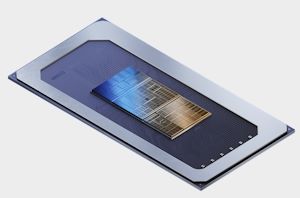
Intel Unveils Meteor Lake Architecture: Intel 4 Heralds the Disaggregated Future of Mobile CPUs
During the opening keynote at Intel's Innovation event in San Jose, Chief Executive Officer Pat Gelsinger unveiled a score of details about the upcoming Meteor Lake client platform. Intel's...
108 by Gavin Bonshor on 9/19/2023
Intel Meteor Lake Client Processors to use Arc Graphics Chiplets
Continuing with this morning’s spate of Intel news coming from Intel’s annual Investor meeting, we also have some new information on Intel’s forthcoming Meteor Lake processors, courtesy of this...
20 by Ryan Smith on 2/17/2022
Intel's Process Roadmap to 2025: with 4nm, 3nm, 20A and 18A?!
In today’s Intel Accelerated event, the company is driving a stake into the ground regarding where it wants to be by 2025. CEO Pat Gelsinger earlier this year stated...
326 by Dr. Ian Cutress on 7/26/2021
Intel to Invest $3.5 Billion USD into Foveros and EMIB Production in Rio Rancho
At a news conference today, Intel has announced that its Rio Rancho campus in New Mexico will be getting an investment of $3.5 billion USD for an expansion of...
20 by Dr. Ian Cutress on 5/3/2021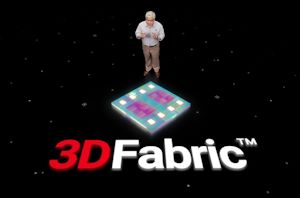
3DFabric: The Home for TSMC’s 2.5D and 3D Stacking Roadmap
Interposers. EMIB. Foveros. Die-to-die stacking. ODI. AIB.TSVs. All these words and acronyms have one overriding feature – they are all involved in how two bits of silicon physically connect...
9 by Dr. Ian Cutress on 9/2/2020
Intel’s Future 7nm FPGAs To Use Foveros 3D Stacking
One of the main battlegrounds of future leading-edge semiconductor products will be in the packaging technology: being able to integrate multiple elements of silicon onto the same package with...
11 by Dr. Ian Cutress on 8/21/2020_carousel.jpg)
Intel Next-Gen 10-micron Stacking: Going 3D Beyond Foveros
One of the issues facing next-generation 3D stacking of chips is how to increase the density of the die-to-die interface. More connections means better data throughput, reducing latency and...
32 by Dr. Ian Cutress on 8/14/2020
The Intel Lakefield Deep Dive: Everything To Know About the First x86 Hybrid CPU
For the past eighteen months, Intel has paraded its new ‘Lakefield’ processor design around the press and the public as a paragon of new processor innovation. Inside, Intel pairs...
225 by Dr. Ian Cutress on 7/2/2020
Intel Discloses Lakefield CPUs Specifications: 64 Execution Units, up to 3.0 GHz, 7 W
Over the past 12 months, Intel has slowly started to disclose information about its first hybrid x86 platform, Lakefield. This new processor combines one ‘big’ CPU core with four...
79 by Dr. Ian Cutress on 6/10/2020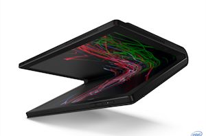
Lenovo’s ThinkPad X1 Fold: Combining Foldable Displays, 5G and Lakefield into a… Laptop?
In 2019 we were exposed to the first foldable display smartphones and wearables, with the Samsung Galaxy Fold, Huawei Mate X, and Xiaomi Mi Mix all demonstrating various themes...
17 by Dr. Ian Cutress on 1/6/2020
An Interconnected Interview with Intel’s Ramune Nagisetty: A Future with Foveros
I’ve constantly stated for the last two years that the next battleground in performance for the semiconductor market is going to be in the interconnect – whether we’re speaking...
19 by Dr. Ian Cutress on 1/3/2020
Intel: Lakefield in 2020, Possible 5G on Foveros
At the IEEE International Electron Devices Meeting (IEDM) 2019, Intel had two package integration presentations, one on its Omni-Directional Interconnect and one on its 3D stacking Foveros technology. In...
37 by Dr. Ian Cutress on 12/11/2019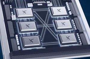
Intel’s Xe for HPC: Ponte Vecchio with Chiplets, EMIB, and Foveros on 7nm, Coming 2021
Today is Intel’s pre-SC19 HPC Devcon event, and with Raja Koduri on stage, the company has given a small glimpse into its high-performance compute accelerator strategy for 2021. Intel...
16 by Dr. Ian Cutress on 11/17/2019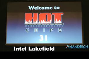
Hot Chips 31 Live Blogs: Intel Lakefield and Foveros
One of the interesting developments in packaging technology in recent memory is the 3D stacking of Intel's new Foveros technology. The first chip to use this packaging technology is...
31 by Dr. Ian Cutress on 8/20/2019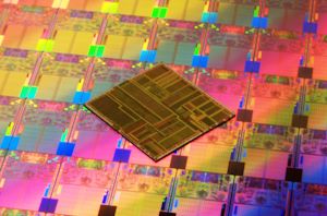
Intel Details Manufacturing through 2023: 7nm, 7+, 7++, with Next Gen Packaging
At Intel's Investor Day today, CEO Bob Swan and Murthy Renduchintala spoke to the ability of the company with respect to its manufacturing capabilities. Intel has historically been strong...
237 by Ian Cutress & Anton Shilov on 5/8/2019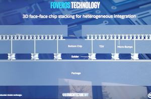
Intel's Interconnected Future: Combining Chiplets, EMIB, and Foveros
While Intel works on getting its main manufacturing process technology on track, it is spending just as much time and effort in researching and developing the rest of the...
117 by Dr. Ian Cutress on 4/17/2019
CES 2019 Quick Bytes: Intel’s 10nm Hybrid x86 Foveros Chip is Called Lakefield
At Intel’s Architecture Day, the company showed off a new stacking technology called ‘Foveros’, which is designed to allows the company to make smaller chips. The idea behind Foveros...
10 by Ian Cutress on 1/7/2019


