The Intel Xeon E7-8800 v3 Review: The POWER8 Killer?
by Johan De Gelas on May 8, 2015 8:00 AM EST- Posted in
- CPUs
- IT Computing
- Intel
- Xeon
- Haswell
- Enterprise
- server
- Enterprise CPUs
- POWER
- POWER8
The Competitor: IBM's POWER8
As we briefly mentioned in the introduction, among all of the potential competitors for the Xeon E7 line, IBM's OpenPower might be the most potent competitor at this time. So how do IBM's offerings compare to Intel's? IBM POWER 8 is a Brainiac (high IPC) design that also wants to be speed demon (high clock speeds).
The POWER8 core can decode, issue and execute and retire 8 instructions per cycle. That degree of of instruction level parallelism (ILP) can not be extracted out of (most) software. To battle the lack of ILP in software, no less than 8 threads (SMT) are active per core. According to IBM,
- 2-threads delivers about 45% performance more than one
- 4-threads deliver yet another 30% boost
- the last 4-threads deliver about 7%
So in total, the 8-way SMT doubles the performance of this massive core. Let us compare the two chips.
| Xeon E7v3/POWER8 Comparison | ||
| Feature | Intel Haswell-EX Xeon E7 |
IBM POWER8 |
| Process tech. | 22nm FinFET | 22nm SOI |
| Max clock | 2.5-3.6 GHz | 3.5-4.35 GHz |
| Max. core count Max. thread count |
18@2.5 GHz 36 SMT |
12@4.2 GHz 96 SMT |
| Max. sustained IPC | 6 (4) | 8 |
| L1-I / L1-D Cache | 32 KB/32 KB | 32 KB/64 KB |
| L2 Cache | 256 KB SRAM per core | 512 KB SRAM per core |
| L3 Cache | 2.5 MB SRAM per core | 8 MB eDRAM per core |
| L4 Cache | None | 16 MB eDRAM per MBC (64/128 MB total) |
| Memory | 1.5 TB per socket (64 GB per DIMM) |
1-2 TB per socket (64 GB per DIMM) |
| Theoretical Memory Bandwidth | 102 GB/s (independent mode) |
204 GB/s |
| PCIe 3.0 Lanes | 40 Lanes | 32 Lanes |
The POWER8 looks better than Haswell-EX in almost every spec, but the devil is of course in the details. First of all, Intel's L2-cache works at the same clock as the core, IBM's L2-cache runs at a lower clock (2.2 GHz or less, depending on the model). Secondly, the POWER8's L3 eDRAM cache might be much larger, but it is so also a bit slower.
But the main disadvantage of the POWER8 is that all this superscalar wideness and high clockspeed goodness comes with a power price. This slide from Tyan at the latest OpenPOWER conference tell us more.
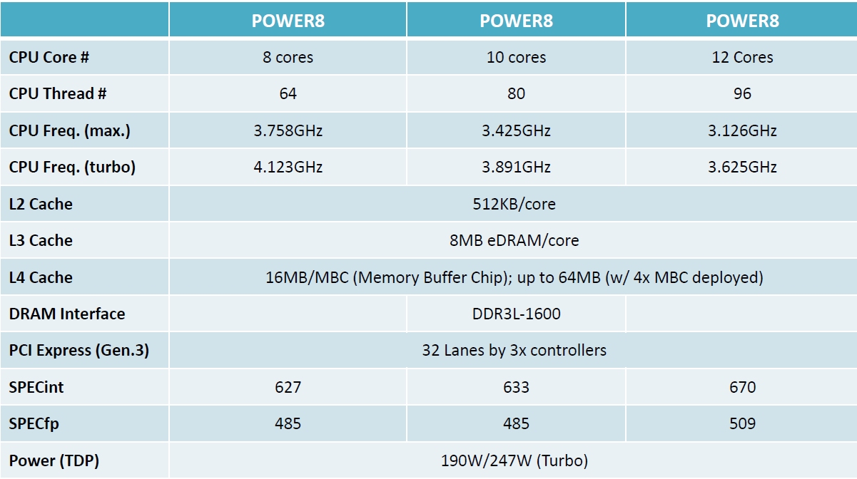
A 12 core POWER8 is "limited" to 3.1 GHz if you want to stay below the 190W TDP mark. Clockspeeds higher than 4 GHz are only possible with 8-cores and a 250W TDP. This makes us really curious what kind of power dissipation we may expect from the 4.2 GHz 10-core POWER8 inside the expensive E870 Enterprise systems (300W?).
That is not all. Each "Jordan Creek2" memory buffer on the Intel system is limited to about 9W. IBM uses a similar but more complex "Centaur" memory buffer (including a 16 MB cache) which needs more than twice as much energy (16-20W). There are at least four of them per chip, and a high-end chip can have eight. So in total the Intel CPU plus memory buffers have a 201W TDP (165W CPU + 4x9W Jordan Creek 2), while the IBM platform has at best a 270W TDP (190W CPU+ 4x20W MBC).


146 Comments
View All Comments
PowerTrumps - Saturday, May 9, 2015 - link
I'm sure the author will update the article unless this was a Intel cheerleading piece.name99 - Friday, May 8, 2015 - link
The thing is called E7-8890. Not E7-5890?WTF Intel? Is your marketing team populated by utter idiots? Exactly what value is there in not following the same damn numbering scheme that your product line has followed for the past eight years or so?
Something like that makes the chip look like there's a whole lot of "but this one goes up to 11" thinking going on at Intel...
name99 - Friday, May 8, 2015 - link
OK, I get it. The first number indicates the number of glueless chips, not the micro-architecture generation. Instead we do that (apparently) with a v2 or v3 suffix.I still claim this is totally idiotic. Far more sensible would be to use the same scheme as the other Intel processors, and use a suffix like S2, S4, S8 to show the glueless SMP capabilities.
ZeDestructor - Friday, May 8, 2015 - link
They've been using this convention since Westmere-EX actually, at which point they ditched their old convention of a prefix letter for power tier, followed by one digit for performance/scalability tier, followed by another digit for generation then the rest for individual models. Now we have 2xxx for dual socket, 4xxx for quad socket and 8xxx for 8+ sockets, and E3/E5/E7 for the scalability tier. I'm fine with either, though I have a slight preference for the current naming scheme because the generation is no longer mixed into the main model number.Morawka - Saturday, May 9, 2015 - link
man the power 8 is a beefy cpu... all that cache, you'd think it would walk all over intel.. but intel's superior cpu design winsPowerTrumps - Saturday, May 9, 2015 - link
please explaintsk2k - Saturday, May 9, 2015 - link
Where are the gaming benchmarks?JohanAnandtech - Saturday, May 9, 2015 - link
Is there still a game with software rendering? :-)Gigaplex - Sunday, May 10, 2015 - link
Llvmpipe on Linux gives a capable (feature wise) OpenGL implementation on the CPU.Klimax - Saturday, May 9, 2015 - link
Don't see POWER getting anywhere with that kind of TDP. There will be dearth of datacenters and other hosting locations retooling for such thing. And I suspect not many will even then take it as cooling and power costs will be damn too high.Problem is, IBM can't go lower with TDP as architecture features enabling such performance are directly responsible for such TDP. (Just L1 consumes 2W to keep few cycles latency at high frequency)