ARM Reveals Cortex-A72 Architecture Details
by Andrei Frumusanu on April 23, 2015 5:00 PM EST- Posted in
- Mobile
- CPUs
- Arm
- Smartphones
- Tablets
- Cortex A72
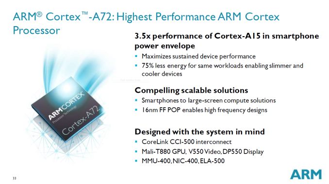
Today in London as part of ARM's TechDay 2015 event we had the pleasure to get a better insight into ARM's new Cortex-A72 CPU. ARM had announced the Cortex-A72 in the beginning of February - leaving a lot of questions to be asked and sense of mystery in the air. The Cortex-A72 is a direct successor to the Cortex-A57 - taking the predecessor as a baseline in order to iterate and improve it.
On the naming side of the equation, moving from 'A57' to 'A72' rather than 'A59' or similar, ARM explains that it is purely a marketing decision as they wanted to give better differentiation between its higher-performance cores from the mid-tier and low-power cores. There seemed to be some confusion between the more power efficienct A53 and the more powerful A57, whereby users would assume they are similar, and thus moving its new big core into the A7x series.
We saw some absolute targeted performance numbers back during the February release, which promised some very interesting numbers that could be achieved over the A57. The problem was that it was not clear how much from performance and power efficiency came from the architectural changes and how much came from the the process on which these targeted performance data points are estimated from. It's clear that on the high-end ARM is promoting the A72 on the new FinFET processes from Samsung/GlobalFoundries and TSMC, which are referred to as 14nm and 16nm in the slides. Generally, due to the design and the node, the A72 will be able to achieve higher clocks than the A57, and we seem to be aiming around 2.5GHz on the 14/16nm nodes when high-end smartphones are concerned. Higher clocks may be present in server applications, where the A72 is also aimed at.

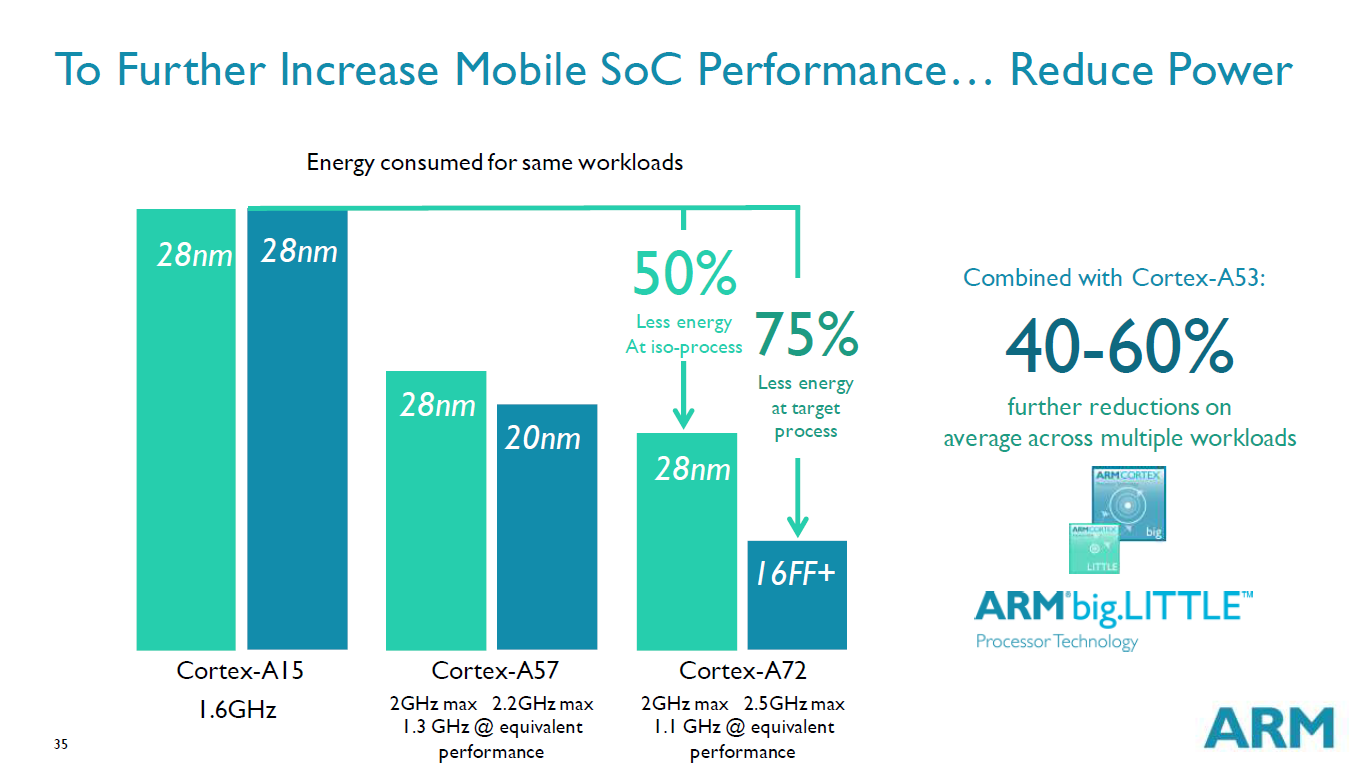
Probably the most interesting slide next to the actual performance metrics of the A72 is the apples-to-apples comparison of the A57 to the A72 on the same process node. When on the 28nm node, we see the A72 having a respectable 20% power reduction when compared to the A57. As a reminder - we're talking about absolute power at the same clock speed, which does not consider performance and thus not a representation of efficiency.
Notably, ARM is aiming for the A72 to be capable of extensive sustained performance at its target frequency. This is something that smaller form factor A57 designs (e.g. phones) have struggled with due to just how powerful A57 is, which has lead to more bursty designs that can only run A57 at its top speeds for short periods of time. We are presented with figures such as sustained 750mW operation per core on 16FF+ at clocks of ~2.5GHz.
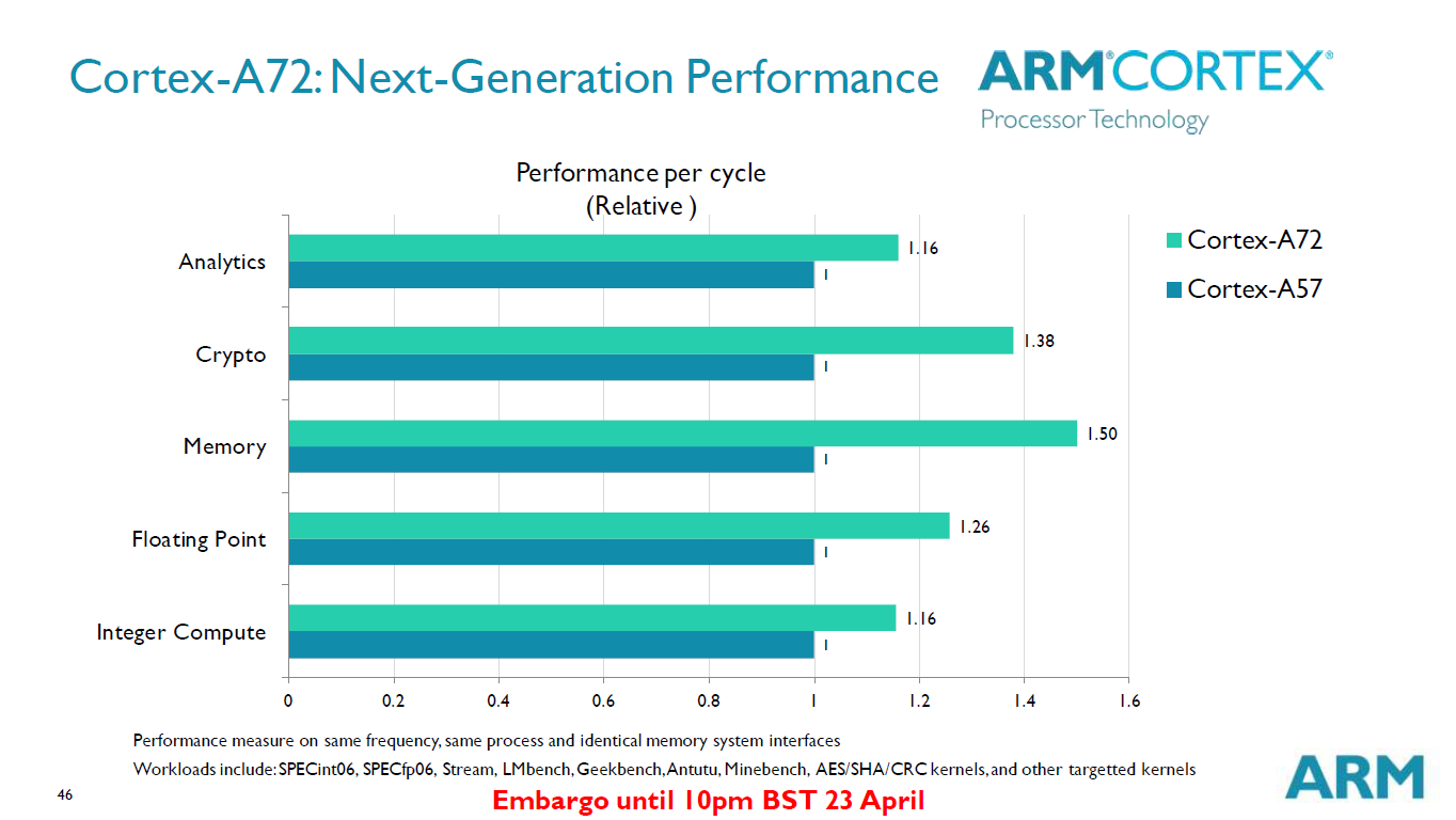
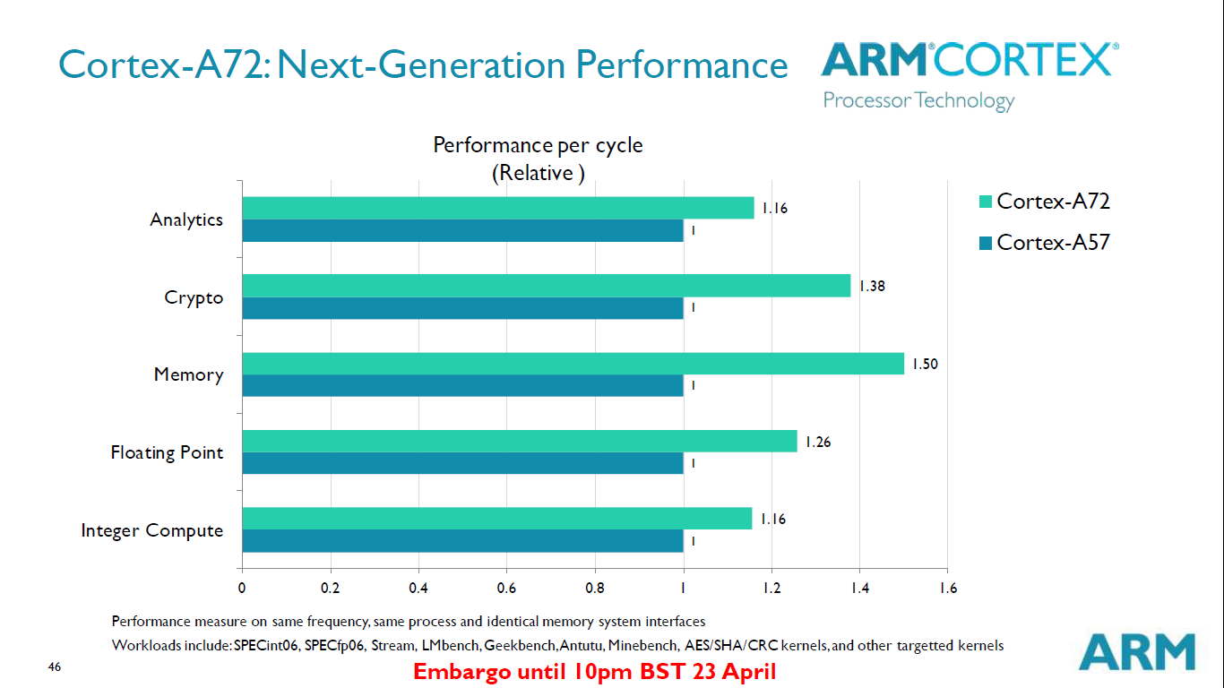
While the power numbers are interesting we also have to put them into context of the achieved work. ARM has made several optimizations to the architecture to improve performance when compared to the A57. We'll get into more detail in just a bit - but what we are looking at is a general 16-30% increase on IPC depending on the kind of workload. Together with the power reduction, we now see how ARM is able to advertise such large efficiency gains for the same fixed workload.
A72 Architecture - The Upgrades Over A57
ARM seems to have managed to achieve an improvement in all three areas of the PPA metric; Performance, Power and Area - the trifecta of semiconductor design goals. This was achieved by doing a re-optimization of (almost) every logical block from the A57. There has been some considerable redesign in the CPU's architecture, some of which include a new branch-predictor and improvements in the decoder pipeline to allows for better throughoutput.

On the level of the instruction fetch block we see a brand new branch-predictor that follows a new sophisticated algorithm that improves performance and reduces power through reduced misprediction and speculation, which has been cut down by 50% for mispredictions and 25% for speculation when compared to the A57. Superfluous branch-predictor accesses have also been suppressed - in workloads where the predictor is not able to do its job efficienctly it is then bypassed completely. There also has been general power optimization in the RAM-organization by coupling the different IP blocks better together, something ARM looks to provide with their own physical IP.
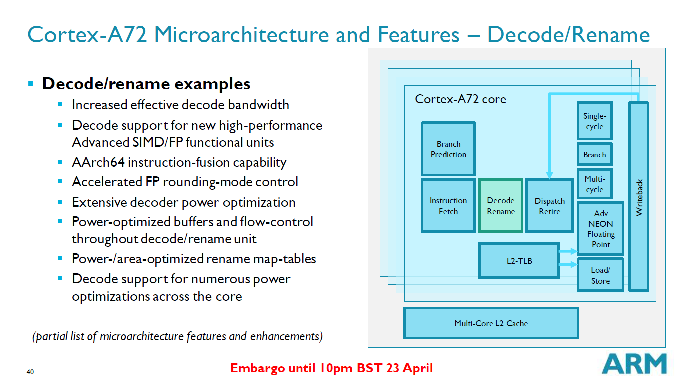
Moving down the pipeline, A72's decoder/rename capabilities have seen their own set of improvements.The decoder itself is still a 3-wide decoder, but ARM has gone through it to try to improve both performance and power consumption in other ways. To improve performance, the effective decode bandwidth has been increased, and the decoder has received some AArch64 instruction-fusion enhancements. Meanwhile power consumption has been tempered at multiple levels, including optimizing decoding directly, and in other power optimizations to the buffers and flow-control hardware that work around the decoder.
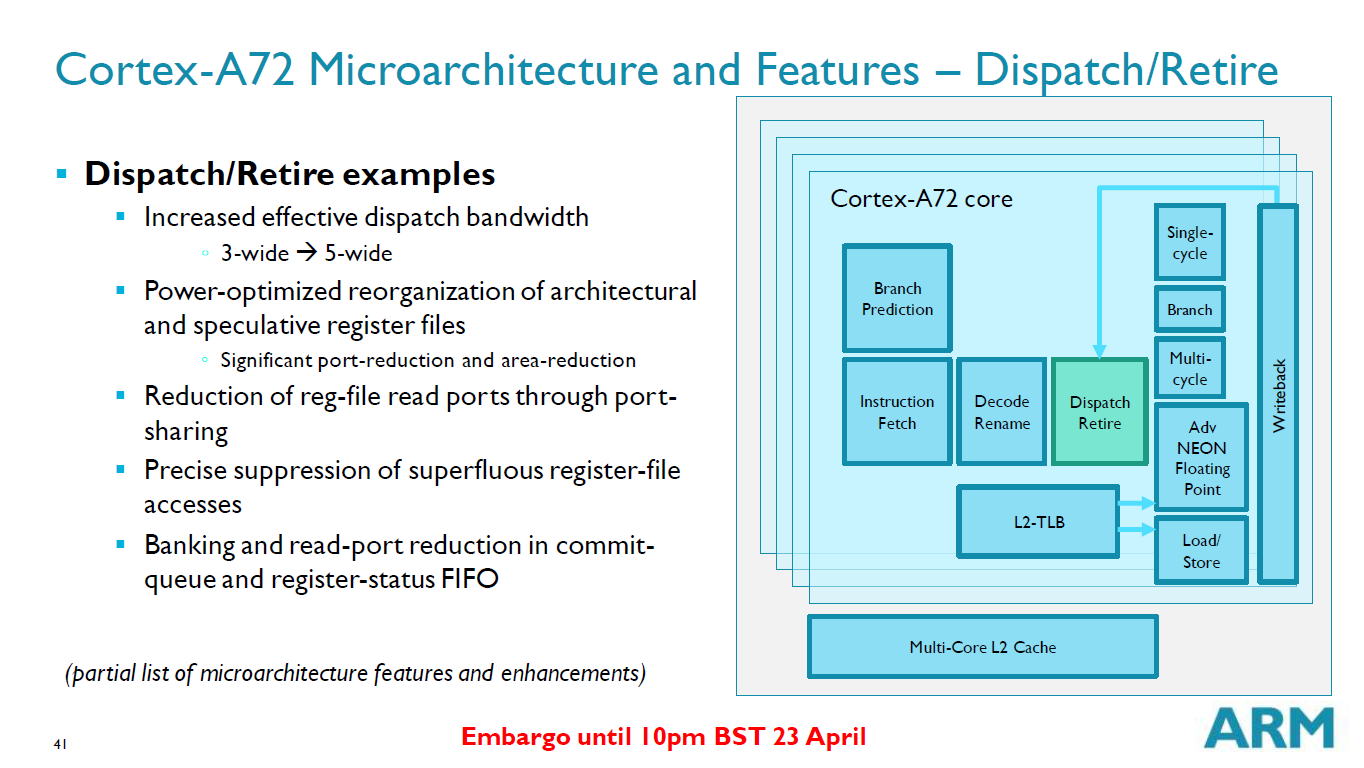
However it's on the dispatch/retire stage that the architecture sees the biggest improvements to performance. Going hand-in-hand with the decoder's ability to fuse instructions, ARM's dispatch unit can then break those ops back down into more granular micro-ops for feeding into the execution units, transforming it from a 3-wide to an effective 5-wide machine at the dispatch stage. The net result of this increases decoder throughput (by reducing the number of individual instructions decoded) while also increasing the total number of micro-ops created by the dispatcher and eventually executed per cycle. ARM is quoting an average of 1.08 micro-ops per instruction in code, which will aid the cases where in A57 the 3-wide dispatch unit was eventually dispatch limited. Again on the dispatch-level, ARM has done more extensive work on their register file by reducing the number of read-ports by introducting port-sharing and further reducing superfluous access.
| ARM CPU Core Comparison | ||||||
| Cortex-A15 | Cortex-A57 | Cortex-A72 | ||||
| ARM ISA | ARMv7 (32-bit) | ARMv8 (32/64-bit) | ||||
| Decoder Width | 3 ops | |||||
| Maximum Pipeline Length | 19 stages | 16 stages | ||||
| Integer Pipeline Length | 14 stages | |||||
| Branch Mispredict Penalty | 15 cycles | |||||
| Integer Add | 2 | |||||
| Integer Mul | 1 | |||||
| Load/Store Units | 1 + 1 (Dedicated L/S) | |||||
| Branch Units | 1 | |||||
| FP/NEON ALUs | 2x64-bit | 2x128-bit | ||||
| L1 Cache | 32KB I$ + 32KB D$ | 48KB I$ + 32KB D$ | ||||
| L2 Cache | 512KB - 4MB | 512KB - 2MB | 512KB - 4MB |
|||
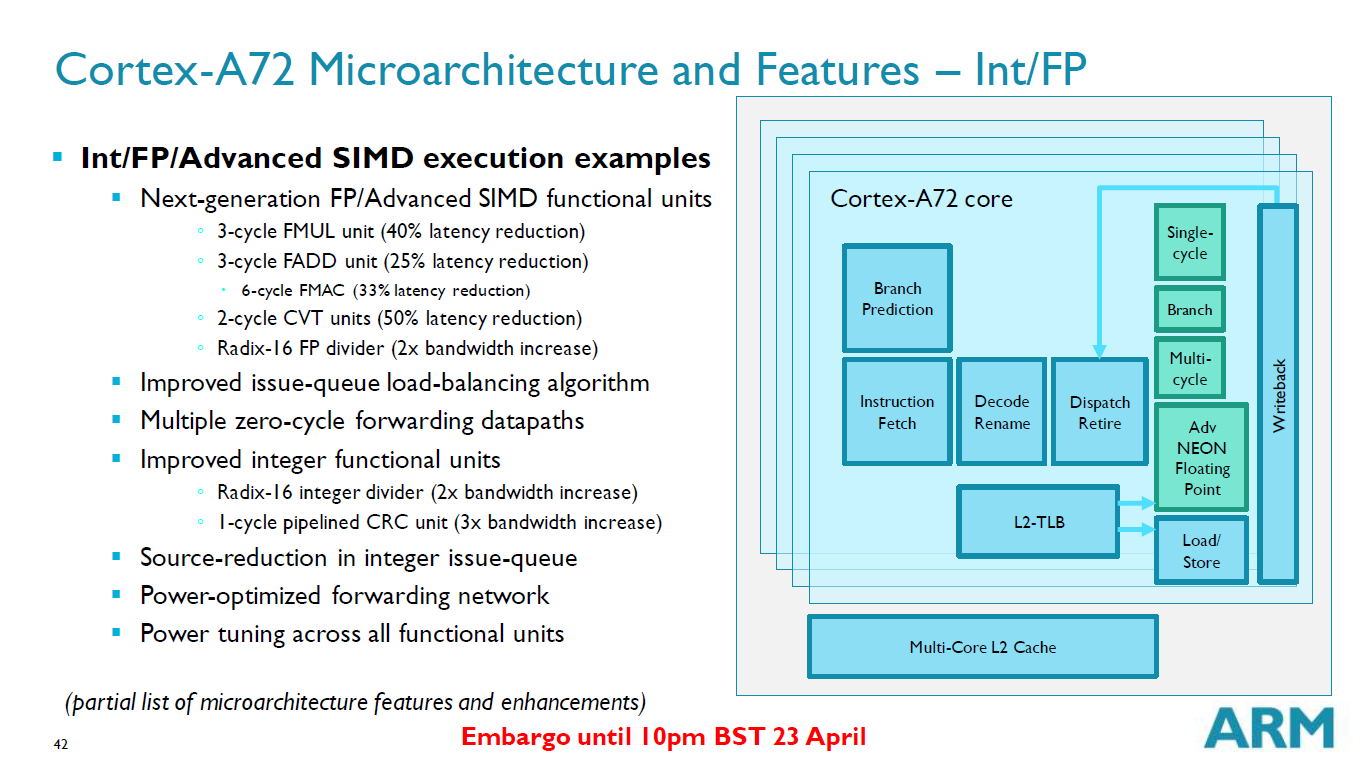
On the side of the execution units we see introduction of new, next-generation FP/Advanced SIMD units. The new units allow for much lower instruction latency as the FP pipeline length is reduced from 9 to 6. FMUL is reduced from 5 cycles down to 3, FADD goes from 4 to 3, FMAC from 9 to 6, and the CVT units go from 4 to 2 units. The reduction of the FP pipeline length brings down the maximum pileline length of the architecture down from 19 to 16.
The integer units also see an improvement, as the Radix-16 divider has seen its bandwidth doubled, while the CRC unit now becomes a pipelined block with just 1-cycle latency, a 3x increase in bandwidth over the A57. Again, we see a repeating pattern here as ARM claims it tried to squeeze the most power efficiency from all the units by improving the physical implementation.
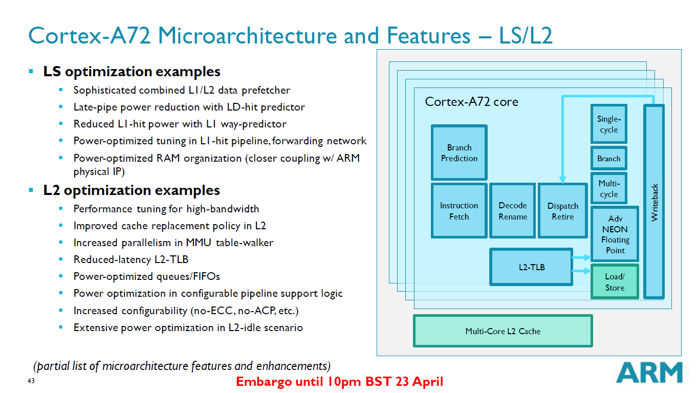
Another large performance improvement over the A57 is found on the Load/Store unit. Here, ARM claims that bandwidth to L1/L2 has been improved by up to 30%. This was achieved by introducting a sophisticated L1/L2 data prefetcher which, again, is at the same time more efficient as improvements in the L1-hit pipeline, fowarding network, and way-predictor reduce the needed power.
We've been generally impressed with what the A72 brings to the table. It's clear that new architecture is an evolutional upgrade ot the A57, and the improvements in performance, power, and area, when looked at from an aggregate view, bring substantial differences and upgrades when compared to the A57. With the A57 having come to market in Q3 of last year and it now shipping in high-volume SoCs such as the Snapdragon 810 and Exynos 7420, we are looking at the possibility of seeing its successor come to market in shipping devices in less than a year's time. The obvious partners that might ramp prodution the soonest are MediaTek and Qualcomm, at least if they are able to hit their target schedules. There should presumably still be un-announced parts from other ARM partners as well. It's clear that ARM has increased the cadence of releasing refreshes of its IP portfolio and the quick succession of the A72 seems to be part of that.
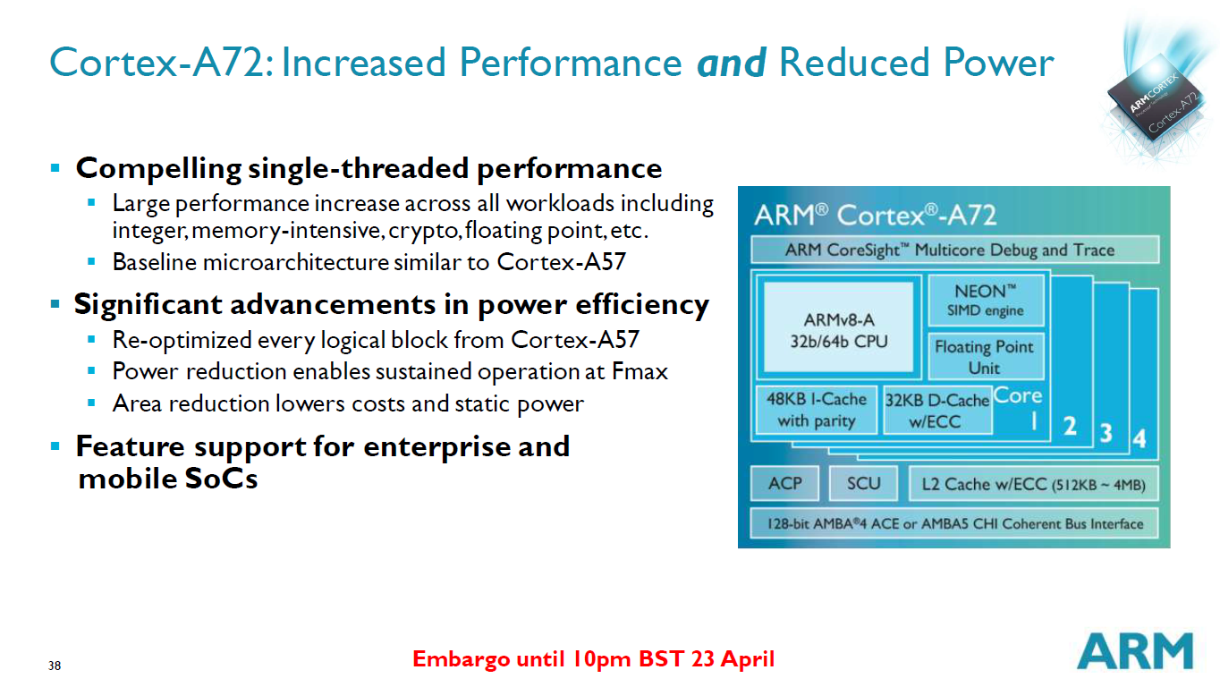
The A72 looks to be a logical update to the A57 addressing some weakpoints such as peak power and power efficiency combined with an ~10% area reduction. We already saw Mediatek showing off an A72 package at MWC, so it will be interesting to see how the IP actually performs in silicon and what ARM's partners will be able to do with the core and the time to market.


92 Comments
View All Comments
mczak - Thursday, April 23, 2015 - link
Well, time to market. Earlier chips are always going to be less optimized than later similar tweaked ones appearing later.Just look at Cortex-A8, if you compare this against Cortex-A7 it is complete junk. Something like twice the die size (at the same process node), but slower (ok similar performance actually), more power hungry, and missing tons of features the Cortex-A7 has (like being MP-capable etc.). But I wouldn't exactly call it a failure :-).
Alexvrb - Thursday, April 23, 2015 - link
Agreed. A57 may have been a stopgap solution, but they needed something to launch sooner - and so did the phone manufacturers. Better to release A57 now and A72 later, than to simply do nothing until A72 rolls around (and piss off big customers who are on a schedule). A57 is certainly better than A15.I'm really looking forward to seeing what the next custom Qualcomm core can do.
hammer256 - Thursday, April 23, 2015 - link
Yeah, you are right. Maybe that time to market pressure was put on by Apple's designs?psychobriggsy - Friday, April 24, 2015 - link
You have to remember that this was ARM's first high-performance (for mobile) 64-bit core. Therefore there were bound to be many areas that could be improved, and I'm sure that internally the A72 refinement process has been going on during the A57 core's final stages of completion.ARM has a history of having multiple revisions of a core design. You'll sometimes see them referenced, e.g., Cortex A15 Revision 3 was used in a Tegra design. These historically improve power consumption, fix bugs, increase performance, etc. This A72 looks to me like a very impressive core revision that's warranted a new marketing name.
tsk2k - Thursday, April 23, 2015 - link
Thanks for the article Andrei.What I'm wondering is if qualcomm will be able to make the snapdragon 820 faster than the snapdragon 620, any thoughts on this?
jjj - Thursday, April 23, 2015 - link
Any clue at all how the cache is scaling on 16/14nm?If it scales poorly it could reach 50% of the quad cluster die area,it wasn't too far in the Exynos 5433 at 46%. It's somewhat strange that cache is using so much die area and not sure how much sense that makes. At this rate Renesas and Cypress will make SRAM with on die CPUs soon not the other way around lol.
hammer256 - Friday, April 24, 2015 - link
Huh, that's weird. So the cache die area isn't shrinking proportionally as other parts? Why would that be? The interconnects?jjj - Friday, April 24, 2015 - link
SRAM doesn't scale all that well.As to why, there are a bunch of factors but i'll let someone more capable on the matter explain it, or you can try to search for some info.
Morawka - Friday, April 24, 2015 - link
SRAM Scales fine but there are trade-off's. see 10nm SSD NANDXtradi - Thursday, April 23, 2015 - link
"...in other power optionizations to the buffers..." What is optionizations ?