The Intel Lakefield Deep Dive: Everything To Know About the First x86 Hybrid CPU
by Dr. Ian Cutress on July 2, 2020 9:00 AM EST
For the past eighteen months, Intel has paraded its new ‘Lakefield’ processor design around the press and the public as a paragon of new processor innovation. Inside, Intel pairs one of its fast peak performance cores with four of its lower power efficient cores, and uses novel technology in order to build the processor in the smallest footprint it can. The new Lakefield design is a sign that Intel is looking into new processor paradigms, such as hybrid processors with different types of cores, but also different stacking and packaging technologies to help drive the next wave of computing. With this article, we will tell you all you need to know about Lakefield.
Part Smartphone, Part PC
When designing a processor, there are over a thousand design choices to be made. The processor can be built to tackle everything, or it can be aimed at a niche. For high performance computing, there might be a need for a high power, high performance design where cooling is of no consideration – compare that to a processor aimed at a portable device, and it needs to be energy efficient and offer considerable battery life for a fixed battery size. There is also the cost of designing the product, how much to invest into research and development, how many units are expected to sell, and thus how many should be produced and what size the product should be. What the price range of the target market is can be a huge factor, even before putting pen to paper.
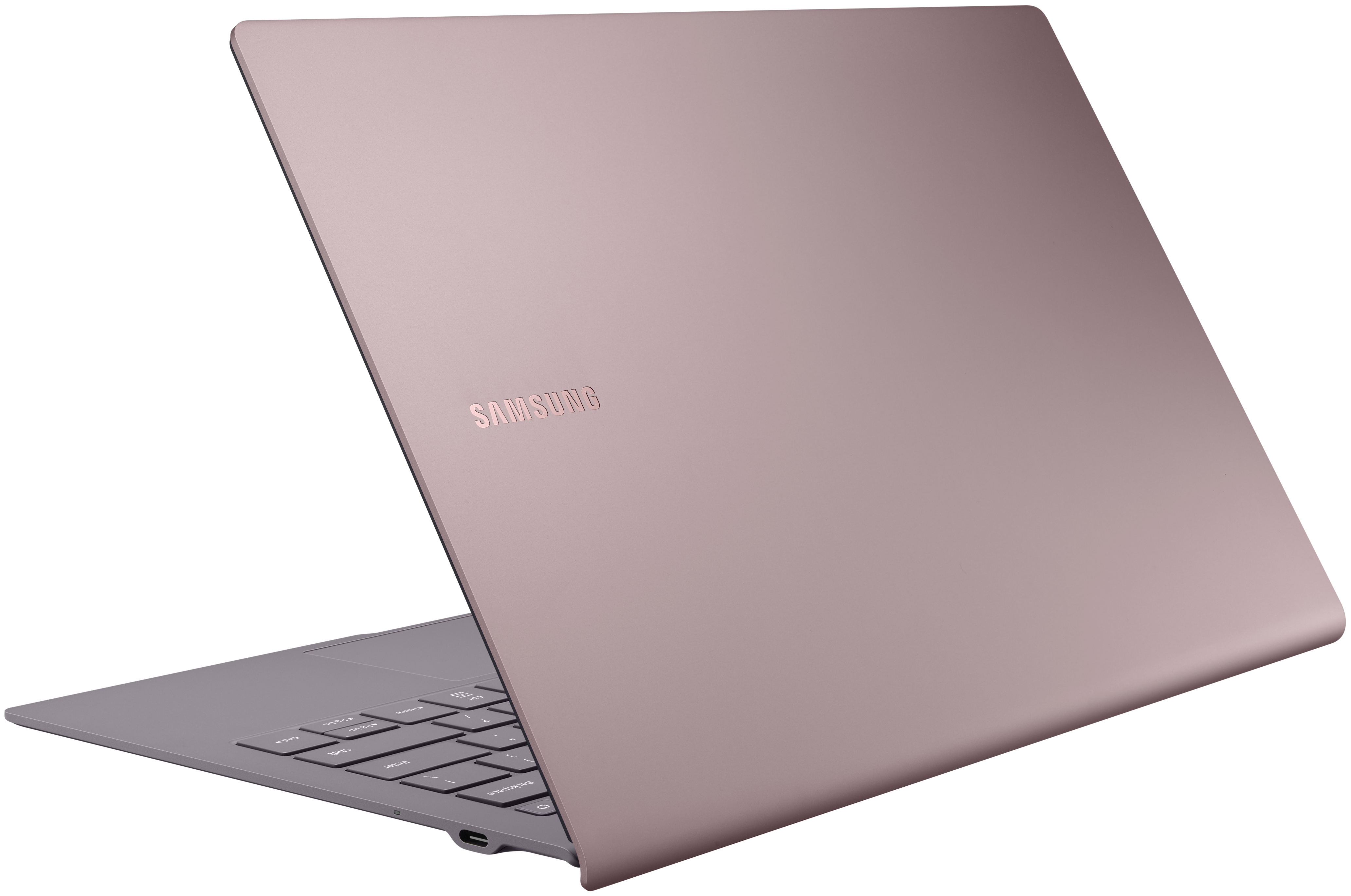
The New Samsung Galaxy Book S
This is all why we have big multi-core processors with lots of compute acceleration in servers, more moderate power and core counts in home machines that focus on single core performance and user experience, and why smartphone processors have to physically fit into a small design and offer exceptional battery life.
Laptop processors have always sort of fit into the middle of the PC and smartphone markets. Laptop users, especially professionals and gamers, need the high performance that a desktop platform can provide, but road warriors need something that is superbly efficient in power consumption, especially at idle, to provide all-day battery life as if they were on a good smartphone. Not only this, but the more energy efficient and the smaller the footprint of the processor and its features, the thinner and lighter the laptop can be, offering a premium design experience.
As a result, we have seen the ultra-premium notebook market converge from two directions.
From the top, we have AMD and Intel, using their laptop processor designs in smaller and smaller power envelopes to offer thin and light devices with exceptional performance and yet retain the energy efficiency required for battery life. For the most premium designs, we see 12-15+ hours of laptop battery life, as well as very capable gaming.
From the bottom, we have Qualcomm, building out its high-performance smartphone processor line into larger power envelopes, in order to offer desktop-class performance with smartphone-class connectivity and battery life. With the designs using Qualcomm’s processors, a user can very easily expect 24+ hours of battery life, and with regular office use, only charge the system once every couple of days. Qualcomm still has an additional barrier in software, which it is working towards.
Both of these directions converge on something in the middle – something that can offer desktop-class performance, 24hr+ battery life, capable gaming, but also has a full range of software support. Rather continue with trying to bring its processors down to the level it requires, Intel has decided to flip its traditional processor paradigm upside down, and build a smartphone-class processor for this market, matching Qualcomm in its bottom up approach while also looking into novel manufacturing techniques in order to do so.
This processor design is called ‘Lakefield’.
Lakefield at the Core, and the Atom
For the past two decades, Intel has had two different types of x86 CPU design.
The Big ‘Core’ CPU
Intel calls its high power/high performance x86 design the ‘Core’ family. This can make it very confusing, to differentiate between the general concept of a processor core and a ‘Core’-based processor core.
Over the years, Core-based processor cores have been designed for power envelopes from low-power laptops all the way up to the beefiest of servers. The Core line of processor cores implement more complex logic in order to provide additional acceleration, at the expense of physical size and power.
The Small ‘Atom’ CPU
The second type of x86 design from Intel is its more energy efficient implementation, called ‘Atom’. With the Atom cores, Intel simplifies the design in order to maximise efficiency for a given power or a given performance. This makes the design smaller, cheaper to manufacturer, but has a lower peak performance than the Core design. We typically see Atom designs in power restricted scenarios where performance is not critical, such as IoT, or low cost laptop designs.
Where Core Meets Atom
Normally we characterise a processor core design in terms of this power and performance. Due to the variation in the design, we see where some designs work best, at various points for a given power or for a given performance. In the case of Intel’s latest generation of Core and Atom hardware, it looks something like this, if we compare one thread against one thread:
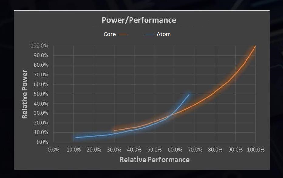
Modified from Intel’s Slides
From this graph, which measures Performance on the bottom axis and power on the side axis, there is a crossover point where each design makes the best sense. When the demand for performance is below 58%, the Atom design is the most power efficient, but above 58% then a Core design is preferred.
Homogenous CPUs (all the same) vs
Heterogeneous CPUs (mix of different)
Now in modern processors, especially in laptops, desktops, and servers, we only experience one type of core design. We either have all Core or all Atom, and the performance is designed to scale within those homogeneous designs. It becomes a simple curve to navigate, and when more parallel performance is required, more of those types of cores are fired up to serve the needs of the end user. This has been the case for these markets for the last 30-50 years.
The smartphone space, for the last decade, has been taking a different approach. Within the smartphone world, there are core designs listed as ‘big’ and core designs listed as ‘little’, in the same way that Intel has Core and Atom designs.
These smartphone processors combine numbers of big cores with numbers of small cores, such that there is an intrinsic benefit to running background tasks on the little cores, where efficiency is important, and user experience related elements on the big cores, where latency and performance is important.
The complexity of such a heterogeneous smartphone-like design has many layers. By default most items will start on the little cores, and it is up to either the processor or the operating system to identify when the higher performance mode during a user experience moment is needed. This can be tricky to identify.
Then also comes the matter when a workload has to actually move from one type of core to the other, typically in response to a request for a specific level of performance – if the cores are designed significantly different, then the demands on the memory can likely increase and it is up to the operating system to ensure everything works as it should. There is also an additional element of security, which is a larger topic outside of the scope of this article.
Ultimately building a design with both big cores and little cores comes down a lot to what we call the scheduler. This is a program inside the operating system that manages where different background processes, user experience events, or things like video editing and games, get arranged. The smartphone market has been working on different types of schedulers, and optimizing the designs, for over a decade as mentioned. For the land of Intel and AMD, the push for heterogeneous schedulers has been a slow process by comparison, and it becomes very much a chicken and egg problem – there is no need for an optimized heterogeneous scheduler if there is never a heterogeneous processor in the market.
So why bring all this up?
Lakefield is the first x86 heterogeneous processor.
In its marketing, Intel calls this a ‘hybrid’ CPU, and we will start to see logos identifying this as such. At the heart of its design, Lakefield combines one of the big Core designs with a cluster of four smaller Atom designs, all into one single piece of silicon. In normal x86 processor talk, this is essentially a ‘penta-core’ design, which will commonly be referred to as a 1+4 implementation (for one big core and four small cores).
Intel’s goal with Lakefield is to combine the benefits of the power efficient Atom core with the better user-experience elements provided by the more power hungry but better peak performing big Core. As a result, it sits in the middle of Intel’s traditional homogeneous designs which only contain one type of x86 design – somewhere above the ‘all Atom’ 0+4 design and somewhere below the ‘all Core’ 4+0 design (in actual fact, it’s closer to 0+4).
Based on our conversations with Intel, and the small demonstrations we have seen so far, the best way to consider the new Lakefield processor is to consider it similar to one of the older quad-core Atom processors, with the benefits of the single core performance of a big Core. The cluster of four smaller Atom CPUs will take care of the heavy lifting and parallel performance requests, because there are four of them, while the big Core will respond when the user loads an application, or touches the screen, or scrolls a web browser.
Being a new form of x86 hybrid CPU is not the only thing that Lakefield brings to the table.

Now, just for some form of clarification, we have already had some experience with these sorts of hybrid CPU designs on operating systems like Windows. Qualcomm’s Windows on Snapdragon laptops, like the Lenovo Yoga, use a 4+4 design with the Snapdragon smartphone chips, and Qualcomm has had to work extensively with Microsoft to develop an appropriate scheduler that can manage workloads between the different CPU designs.
The main difference to what Qualcomm has done and what Intel is doing with Lakefield is in software support – Qualcomm processors run ‘Arm’ instructions, while Intel processors run ‘x86’ instructions. Most Windows software is built for x86 instructions, which has limited Qualcomm’s effectiveness in penetrating the traditional laptop market. Qualcomm's design actually allows for ‘x86 translation’, however its scope is limited and there is a performance penalty, but is a work in progress. The point being is that while we have not had a hybrid CPU scheduler for Windows on an x86 system previously, there has been a lot of work put in by Microsoft to date while working with Qualcomm.
Visualising Heterogeneous CPU Designs
Not to any sort of scale
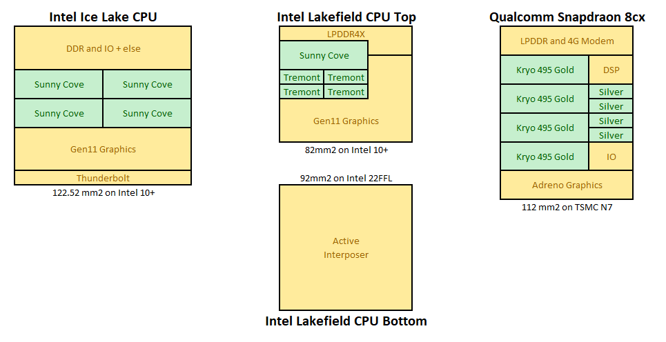
Here are some examples of mobile processors, from Intel and Qualcomm, with the cores in green. On the left is Intel's own Ice Lake processor, with four big cores. In the middle is Intel's Lakefield, which has two stacked silicon dies, but it's the top one that has one big core and four small ones. On the right is Qualcomm's Snapdragon 8cx, currently used in Windows on Snapdragon devices, which uses four performance cores and four efficiency cores, but also integrates a smartphone modem onboard.
In this article, over the following pages, we'll be looking at Intel's new Lakefield processor in detail, covering the new multi-core design, discussing chiplets and Intel's new die-to-die bonding technology called Foveros, the implications of such a design on laptop size (as well as looking at the publicly disclosed Lakefield laptops coming to market), die shots, supposed performance numbers, thermal innovations, and the future for Lakefield. Data for this article has come from our research as well as interviews with Intel's technical personnel and Intel's own presentations on Lakefield at events such as HotChips, Architecture Day, CES, IEDM, and ISSCC. Some information is dissected with helpful input from David Schor of Wikichip. We also cover some of Intel’s innovations with the scope of other semiconductor companies, some of which may be competitors.


221 Comments
View All Comments
PaulHoule - Saturday, July 4, 2020 - link
@DrK,the engineering on this part is like what you'd get if you contracted out to Rockwell or Litton Industries for a brain for a Stinger missile. Compact, brilliantly packaged, with adequate performance, but no concern at all about thermal dissipation because the missile is going to hit or miss its target before the CPU fries.
Foveros is an expensive technology for a mass market device (cheap tablet) because the fabrication cost depends on the total area and there is an expensive step of stitching the chips together at the end. If you could avoid fabricating "glue" components and just snap together chips from a library this might be an amazing technology to build 500 of something at low development cost and time (e.g. weeks) If you have to make a new mask for the chip, however, it is a lot less fun.
So far as AVX the problem is as you say: "who cares about AVX?" Intel has shipped a backlog of features that people don't use because of overhead and complexity. As a software dev I get paid to work on certain aspect of my products, and maximizing performance with the latest instructions may or may not be on my agenda. If it is easy to do I will push for it but it means debugging compatibility problems it is a tough ask. "Optimal" performance for a range of users can mean shipping many versions of a function; the performance of loading, installing, updating, those libraries will be not in the least optimal.
Intel is like that Fatboy Slim album, 'We're #1, Why Try Harder?' The world has changed and Intel is not the #1 CPU firm any more. Intel has to get more Paranoid or it might not Survive.
Spunjji - Monday, July 6, 2020 - link
Why start with "I'm not one to criticise" and then do it? Clearly you are, and as a rhetorical flourish it's tedious in the extreme.1 - It's a first-gen product and it shows, but they're putting it in premium products.
2 - No deep-dive, for sure, but Intel's own figures are not very encouraging.
3 - Citation needed here. There's no sign of it being used outside of low-power premium devices.
4 - Who cares about AVX indeed! Tell that to the Intel fanboys pissing all over the AMD threads?
I'm entirely in favour of your final conclusion, but it's not really supported by the previous statements. 🤷♂️
Oxford Guy - Friday, July 3, 2020 - link
Bricklake or bust.Meteor2 - Friday, July 3, 2020 - link
Ultimately this is another attempt by Intel to stay relevant in a space where it's always struggled: mobile. With the progress being made by Apple, Microsoft, and Qualcomm using ARM, Intel is looking at losing an ever-growing chunk of what was the laptop market.But whatever Intel tries, bottom line is that ARM is more efficient than x86.
Beaver M. - Friday, July 3, 2020 - link
Thats not the issue. The issue is that theres not much software in that sector for x86.Valantar - Sunday, July 5, 2020 - link
A few errors in the article: 2 16-bit channels of LPDDR4X should be 2 32-bit channels of LPDDR4X, given that Renoir (with 4 32-bit LP4X channels at the same clock speed) delivers exactly 2x the bandwidth. Right?You should also proofread the pasted-in laptop descriptions; a lot of stuff in them clashes with the previous text.
Beyond that though: great article! Part of the reason why I love AT is for these technical yet understandable deep-dives. Looking forward to the next one.
Pixelpusher6 - Sunday, July 5, 2020 - link
Interesting choice to place the DRAM right over the core, seems like it would make more sense to move it next to the chip but on package. I guess my question is was it worth the complexity to implement this Foveros design to save a little space? It seems like they could have gotten the same benefit by using a traditional packaging i.e. with a little large package. Can you imagine paying $2500 like the price of that Lenovo and having Atom-esque performance?Pixelpusher6 - Sunday, July 5, 2020 - link
*largerFarfolomew - Monday, July 6, 2020 - link
Agreed on the DRAM placement. It seems really out of place. Another "dime size" piece of silicon right next to the Lakefield CPU doesn't seem like it would take up much more board space, and would alleviate a ton of the heat dissipation problems by allowing the compute-layer die to be directly connected to a heatsinkserendip - Monday, July 6, 2020 - link
It seems to be an interesting technical answer to a question nobody asked. Board space is a lot cheaper than what Lakefield would cost. It could also cost more for Intel to produce and they'd be stuck carrying multiple RAM SKUs.Heat dissipation could be a major issue. The slow chip could become even slower if it has to constantly throttle down because of thermal loads. Intel is sadly mistaken if this is supposed to be an ARM competitor.