Intel Launches Cooper Lake: 3rd Generation Xeon Scalable for 4P/8P Servers
by Dr. Ian Cutress on June 18, 2020 9:00 AM ESTSocket, Silicon, and SKUs
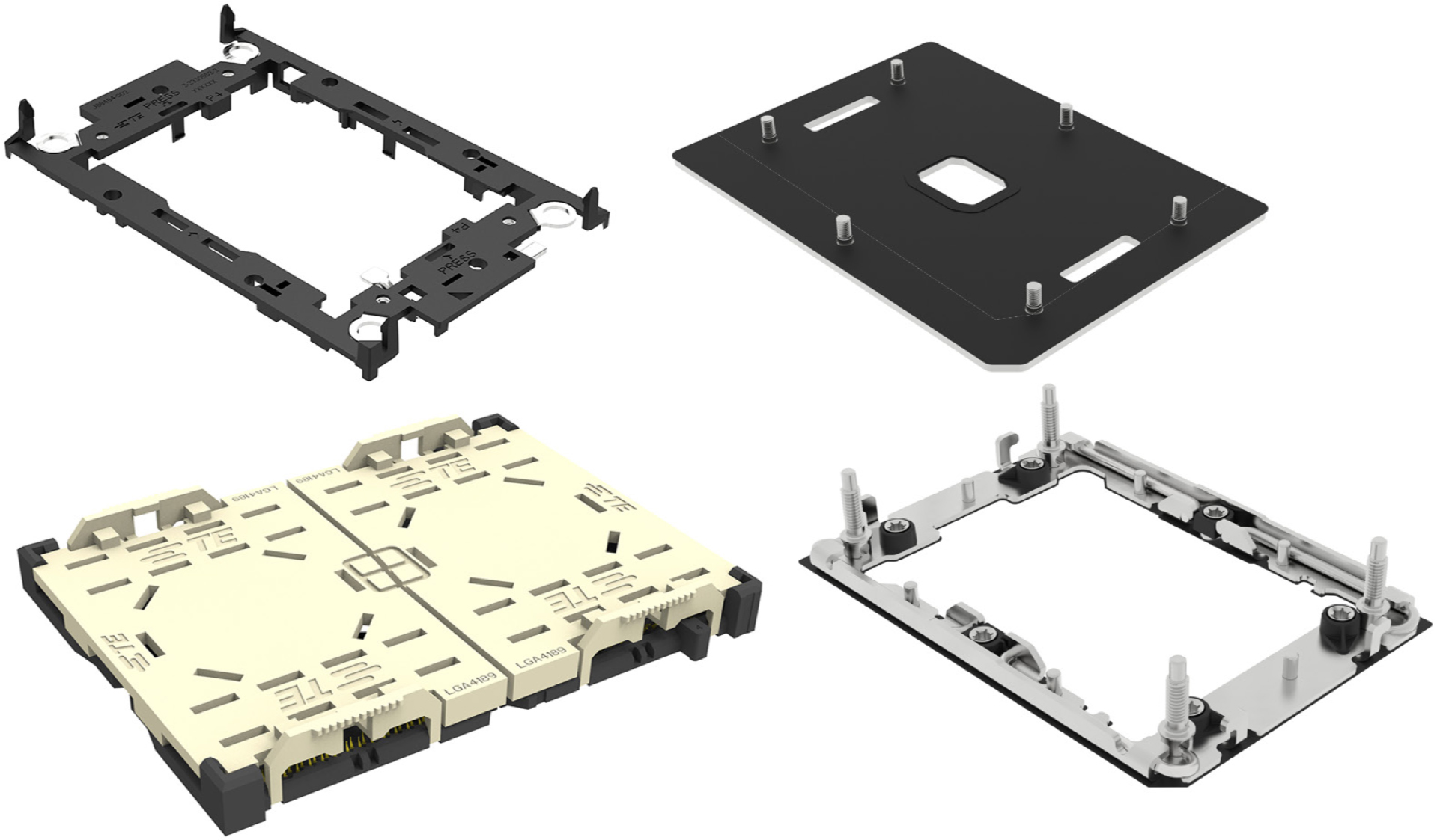
Cooper Lake Xeon Scalable ushers in a new socket, given that it is difficult to add in UPI links without adding additional pins. The new socket is known as LGA4189, for which there will be two variants: LGA4189-4 and LGA4189-5. When asked, Intel stated that Cooper Lake supports the LGA4189-5 socket, however when we asked an OEM about the difference between the sockets, we were told it comes down to the PCIe version.
LGA4189-5, for Cooper Lake, uses PCIe 3.0. LGA4189-4, which is for Ice Lake we were told, will be PCIe 4.0 Nonetheless, Intel obfuscates the difference by calling both of them ‘Socket P+’. It’s not clear if they will be interchangeable, given that technically PCIe 4.0 can work in PCIe 3.0 mode, and a PCIe 3.0 chip can work in a PCIe 4.0 board at PCIe 3.0 speeds, but it will come down to how the UPI links are distributed, and any other differences.
We've since been told that the design of the socket is meant to make sure that Ice Lake Xeon processors should not be placed in Cooper Lake systems, however Cooper Lake processors will be enabled in systems built for Ice Lake.
We’re unsure if that means that LGA4189 / Socket P+ will be a single generation socket or not. Sapphire Rapids, mean to be the next generation Xeon Scalable, is also set for 2nd gen Optane support, which could imply a DDR4 arrangement. If Sapphire Rapids supports CXL, then that’s a PCIe 5.0 technology. There’s going to be a flurry of change within Intel’s Xeon ecosystem it seems.
On the silicon side, Intel has decided to not disclose the die configurations for Cooper Lake. In previous generations of Xeon and Xeon Scalable, Intel would happily publish that it used three different die sizes at the silicon level to separate up the core count distribution. For Cooper Lake however, we were told that ‘we are not disclosing this information’.
I quipped that this is a new level of secrecy from Intel.
Given that Cooper Lake will be offered in variants from 16 to 28 cores, and is built on Intel’s 14nm class process (14+++?), we can at least conclude there is a ’28 core XCC’ variant. Usually on these things the L3 cache counts are a good indicator of something smaller is going to be part of the manufacturing regime, however each processor sticks to the 1.375 MB of L3 cache per core configuration.
This leads us onto the actual processors being launched. Intel is only launching Platinum 8300, Gold 6300, and Gold 5300 versions of Cooper Lake, given that its distribution is limited to four socket systems or greater, and to high scale OEMs only. TDPs start at 150-165 W for the 16-24 core parts, moving up to 205-250 W for the 18-28 core parts. The power increases come from a combination of slight frequency bumps, higher memory speed support, and double the UPI links.
| Intel 3rd Gen Xeon Scalable Cooper Lake 4P/8P |
||||||||||
| AnandTech | Cores | Base Freq |
1T Turbo |
DDR4 1DPC |
DDR4 2DPC |
DDR4 TiB |
TDP W |
4P 8P |
Intel SST |
Price |
| Xeon Platinum 8300 | ||||||||||
| 8380HL | 28C | 2900 | 4300 | 3200 | 2933 | 4.5 | 250 | 8P | No | $13012 |
| 8380H | 28C | 2900 | 4300 | 3200 | 2933 | 1.125 | 250 | 8P | No | $10009 |
| 8376HL | 28C | 2600 | 4300 | 3200 | 2933 | 4.5 | 205 | 8P | No | $11722 |
| 8376H | 28C | 2600 | 4300 | 3200 | 2933 | 1.12 | 205 | 8P | No | $8719 |
| 8354H | 18C | 3100 | 4300 | 3200 | 2933 | 1.12 | 205 | 8P | No | $3500 |
| 8353H | 18C | 2500 | 3800 | 3200 | 2933 | 1.12 | 150 | 8P | No | $3003 |
| Xeon Gold 6300 | ||||||||||
| 6348H | 24C | 2300 | 4200 | - | 2933 | 1.12 | 165 | 4P | No | $2700 |
| 6328HL | 16C | 2800 | 4300 | - | 2933 | 4.5 | 165 | 4P | Yes | $4779 |
| 6328H | 16C | 2800 | 4300 | - | 2933 | 1.12 | 165 | 4P | Yes | $1776 |
| Xeon Gold 5300 | ||||||||||
| 5320H | 20C | 2400 | 4200 | - | 2933 | 1.12 | 150 | 4P | Yes | $1555 |
| 5318H | 18C | 2500 | 3800 | - | 2933 | 1.12 | 150 | 4P | No | $1273 |
| All CPUs have Hyperthreading | ||||||||||
Quite honestly, Intel's naming scheme is getting more difficult to follow. Every generation of Xeon Scalable becomes a tangled mess of feature separation.
No prices are attached to any of the Cooper Lake processors from our briefings, but Intel did publish them in its price document. We can compare the top SKUs from the previous generations, as well as against AMD's best.
| Intel Xeon 8x80 Compare | ||||
| Xeon 8180M |
Xeon 8280L |
Xeon 8380HL |
AnandTech | EPYC 7H12 |
| Skylake | Cascade | Cooper | Platform | Rome |
| 14nm | 14+ nm | 14++ nm? | Node | 7nm + 14nm |
| $13011 | $13012 | $13012 | Price | ~$8500 |
| 28 C | 28 C | 28 C | Cores | 64 C |
| 2500 MHz | 2700 MHz | 2900 MHz | Base | 2600 MHz |
| 3800 MHz | 4000 MHz | 4300 MHz | 1T Turbo | 3300 MHz |
| 6 x 2666 | 6 x 2933 | 6 x 3200 | DDR4 | 8 x 3200 |
| 1.5 TiB DDR4 | 4.5 TiB Optane | 4.5 TiB Optane | Max Mem | 4 TiB DDR4 |
| 205 W | 205 W | 250 W | TDP | 280 W |
| 1P to 8P | 1P to 8P | 1P to 8P | Sockets | 1P, 2P |
| 3 x 10.4 GT/s | 3 x 10.4 GT/s | 6 x 10.4 GT/s | UPI/IF | 64 x PCIe 4.0 |
| 3.0 x48 | 3.0 x48 | 3.0 x48 | PCIe | 4.0 x128 |
| AVX-512 F/CD/BW/DQ |
AVX-512 F/CD/BW/DQ + VNNI |
AVX-512 F/CD/BW/DQ + VNNI +BF16 |
AVX | AVX2 |
The new processor improves on base frequency by +200 MHz and turbo frequency by +300 MHz, but it does have that extra 45 W TDP.
Compared to AMD’s Rome processors, the most obvious advantages to Intel are in frequency socket support, the range of vector extensions supported, and also memory capacity if we bundle in Optane. AMD’s wins are in has core counts, price, interconnect, PCIe count, and memory bandwidth. However, the design of Intel’s Cooper Lake with BF16 support is ultimately for customers who weren’t looking at AMD for those workloads.
We should also point out that these SKUs are the only ones Intel is making public. As explained in previous presentations, more than 50% of Intel's Xeon sales are actually custom versions of these, with different frequency / L3 cache / TDP variations that the big customers are prepared to pay for. In Intel's briefing, some of the performance numbers given by its customers are based on that silicon, e.g. 'Alibaba Customized SKU'. We never tend to hear about these, unfortunately.
Platform
As hinted above, Intel is still supporting PCIe 3.0 with Cooper Lake, with 48 lanes per CPU. The topology will also reuse Intel’s C620 series chipsets, providing 20 more lanes of PCIe 3.0 as well as USB 3.0 and SATA.
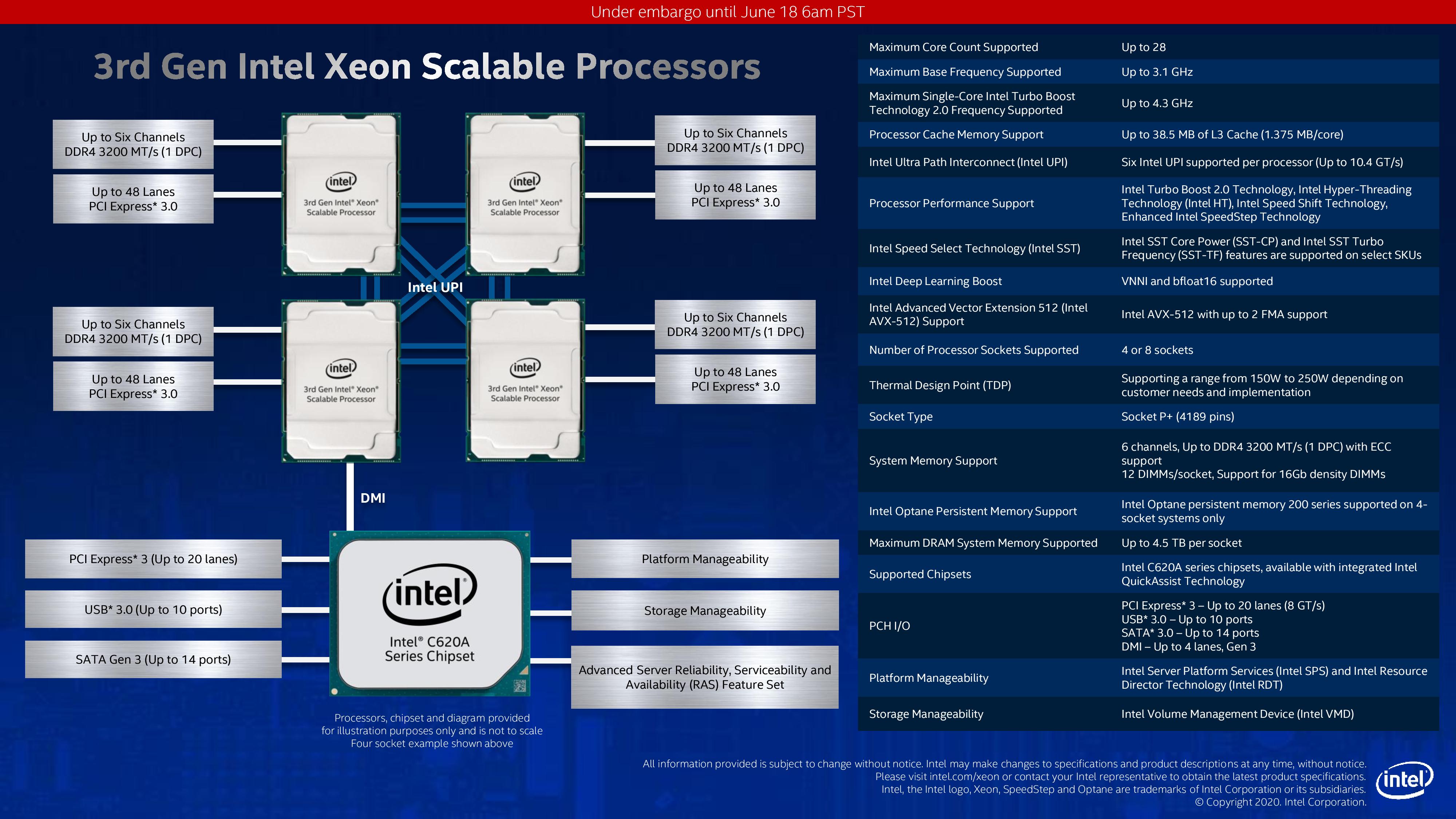
Intel did not go into items such as VROC support or improvements for this generation, so we expect support for those to be similar to Cascade Lake.


99 Comments
View All Comments
schujj07 - Saturday, June 20, 2020 - link
What proof do you have for any of those claims. Please link actual sources instead of your own thoughts.Korguz - Saturday, June 20, 2020 - link
schujj07, you know he doesnt have ANY proof of this FUD he keeps spitting out. and he will NEVER post any proof what so ever of it. his posts, are 100% his own thoughts, misinformation, and FUD, specially if it means he has a chance to bash amd, and praise his gods intel and nvidia.schujj07 - Saturday, June 20, 2020 - link
I know he doesn't have proof. I just want to see if he will try or just give up.Korguz - Sunday, June 21, 2020 - link
he will just run away and hide, like he always does when someone calls him out on his made up fud, or, resort to his usual name calling, insults and condescending remarksDeicidium369 - Thursday, June 25, 2020 - link
https://www.quora.com/Why-is-Intel-pursuing-Cobalt...https://semiwiki.com/semiconductor-manufacturers/i...
https://semiengineering.com/dealing-with-resistanc...
Pretty simple to Google - http://www.google.com type in what you are searching for.
Deicidium369 - Saturday, June 20, 2020 - link
Intel 10nm+ is roughly equal to TSMC "7nm"LMAO - so no, no where near 5-7 years - stick to flipping burgers.
Korguz - Saturday, June 20, 2020 - link
" stick to flipping burgers. " like you used to do before you were layed off from McDonalds?Deicidium369 - Thursday, June 25, 2020 - link
So clever. Wow, your massive intellect has beaten me. Oh what shall I do.WuMing2 - Tuesday, July 7, 2020 - link
Shall we use 14+X6 to keep track of Intel manufacturing process updates? To be clear this is the sixt iteration of 14nm process introduced in 2014. And God save the Queen.