NVIDIA Ampere Unleashed: NVIDIA Announces New GPU Architecture, A100 GPU, and Accelerator
by Ryan Smith on May 14, 2020 9:00 AM EST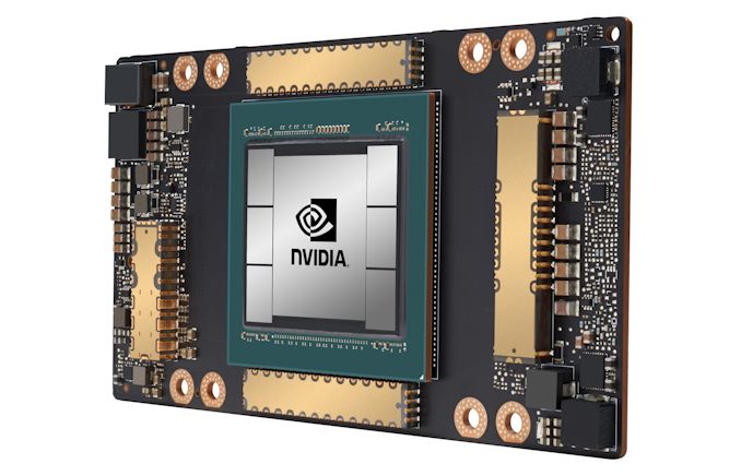
While NVIDIA’s usual presentation efforts for the year were dashed by the current coronavirus outbreak, the company’s march towards developing and releasing newer products has continued unabated. To that end, at today’s now digital GPU Technology Conference 2020 keynote, the company and its CEO Jensen Huang are taking to the virtual stage to announce NVIDIA’s next-generation GPU architecture, Ampere, and the first products that will be using it.
Like the Volta reveal 3 years ago – and is now traditional for NVIDIA GTC reveals – today’s focus is on the very high end of the market. In 2017 NVIDIA launched the Volta-based GV100 GPU, and with it the V100 accelerator. V100 was a massive success for the company, greatly expanding their datacenter business on the back of the Volta architecture’s novel tensor cores and sheer brute force that can only be provided by a 800mm2+ GPU. Now in 2020, the company is looking to continue that growth with Volta’s successor, the Ampere architecture.
Now a much more secretive company than they once were, NVIDIA has been holding its future GPU roadmap close to its chest. While the Ampere codename (among others) has been floating around for quite some time now, it’s only this morning that we’re finally getting confirmation that Ampere is in, as well as our first details on the architecture. Due to the nature of NVIDIA’s digital presentation – as well as the limited information given in NVIDIA’s press pre-briefings – we don’t have all of the details on Ampere quite yet. However for this morning at least, NVIDIA is touching upon the highlights of the architecture for its datacenter compute and AI customers, and what major innovations Ampere is bringing to help with their workloads.
Kicking things off for the Ampere family is the A100. Officially, this is the name of both the GPU and the accelerator incorporating it; and at least for the moment they’re both one in the same, since there is only the single accelerator using the GPU.
| NVIDIA Accelerator Specification Comparison | |||||
| A100 | V100 | P100 | |||
| FP32 CUDA Cores | 6912 | 5120 | 3584 | ||
| Boost Clock | ~1.41GHz | 1530MHz | 1480MHz | ||
| Memory Clock | 2.4Gbps HBM2 | 1.75Gbps HBM2 | 1.4Gbps HBM2 | ||
| Memory Bus Width | 5120-bit | 4096-bit | 4096-bit | ||
| Memory Bandwidth | 1.6TB/sec | 900GB/sec | 720GB/sec | ||
| VRAM | 40GB | 16GB/32GB | 16GB | ||
| Single Precision | 19.5 TFLOPs | 15.7 TFLOPs | 10.6 TFLOPs | ||
| Double Precision | 9.7 TFLOPs (1/2 FP32 rate) |
7.8 TFLOPs (1/2 FP32 rate) |
5.3 TFLOPs (1/2 FP32 rate) |
||
| INT8 Tensor | 624 TOPs | N/A | N/A | ||
| FP16 Tensor | 312 TFLOPs | 125 TFLOPs | N/A | ||
| TF32 Tensor | 156 TFLOPs | N/A | N/A | ||
| Interconnect | NVLink 3 12 Links (600GB/sec) |
NVLink 2 6 Links (300GB/sec) |
NVLink 1 4 Links (160GB/sec) |
||
| GPU | GA100 (826mm2) |
GV100 (815mm2) |
GP100 (610mm2) |
||
| Transistor Count | 54.2B | 21.1B | 15.3B | ||
| TDP | 400W | 300W/350W | 300W | ||
| Manufacturing Process | TSMC 7N | TSMC 12nm FFN | TSMC 16nm FinFET | ||
| Interface | SXM4 | SXM2/SXM3 | SXM | ||
| Architecture | Ampere | Volta | Pascal | ||
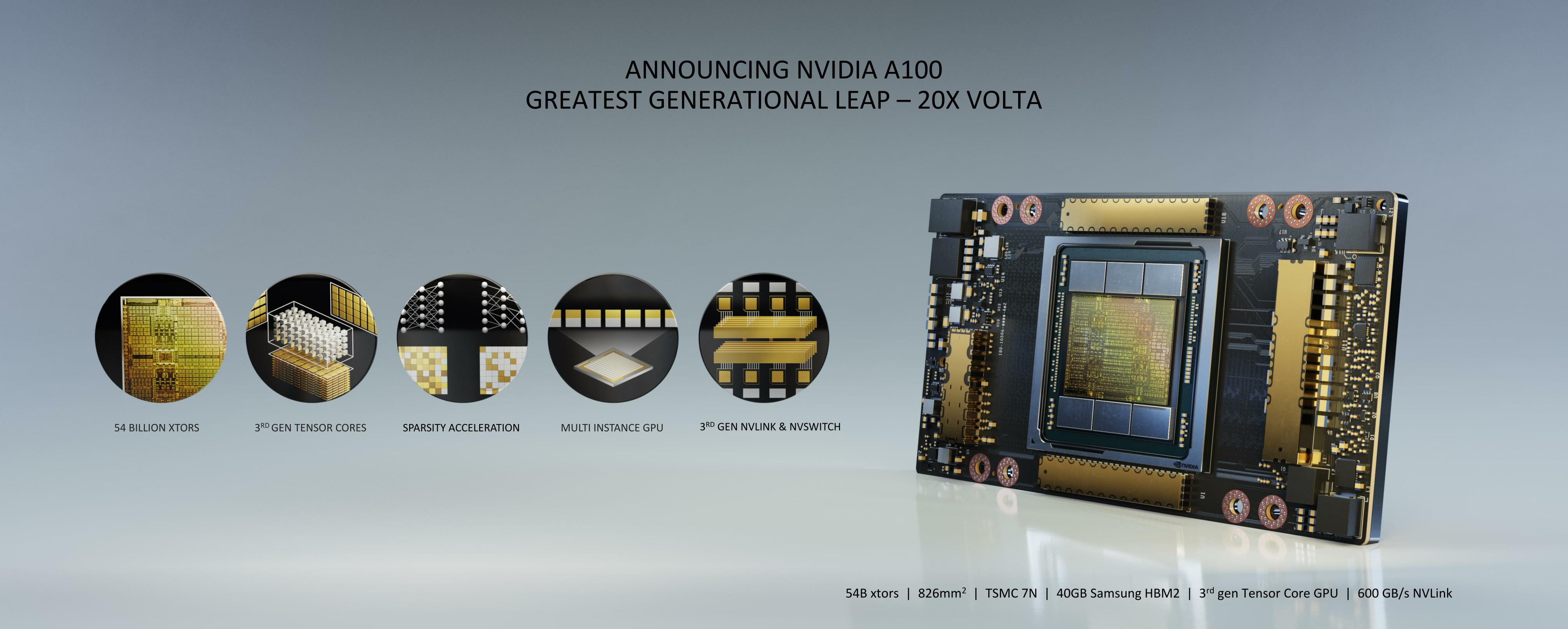
Designed to be the successor to the V100 accelerator, the A100 aims just as high, just as we’d expect from NVIDIA’s new flagship accelerator for compute. The leading Ampere part is built on TSMC’s 7nm process and incorporates a whopping 54 billion transistors, 2.5x as many as the V100 before it. NVIDIA has put the full density improvements offered by the 7nm process in use, and then some, as the resulting GPU die is 826mm2 in size, even larger than the GV100. NVIDIA went big on the last generation, and in order to top themselves they’ve gone even bigger this generation.
We’ll touch more on the individual specifications a bit later, but at a high level it’s clear that NVIDIA has invested more in some areas than others. FP32 performance is, on paper, only modestly improved from the V100. Meanwhile tensor performance is greatly improved – almost 2.5x for FP16 tensors – and NVIDIA has greatly expanded the formats that can be used with INT8/4 support, as well as a new FP32-ish format called TF32. Memory bandwidth is also significantly expanded, with multiple stacks of HBM2 memory delivering a total of 1.6TB/second of bandwidth to feed the beast that is Ampere.
NVIDIA will be delivering the initial version of this accelerator in their now-common SXM form factor, which is a mezzanine-style card well-suited for installation in servers. On a generation-over-generation basis, power consumption has once again gone up, which is probably fitting for a generation called Ampere. Altogether the A100 is rated for 400W, as opposed to 300W and 350W for various versions of the V100. This makes the SXM form factor all the more important for NVIDIA’s efforts, as PCIe cards would not be suitable for that kind of power consumption.
As for the Ampere architecture itself, NVIDIA is releasing limited details about it today. Expect we’ll hear more over the coming weeks, but for now NVIDIA is confirming that they are keeping their various product lines architecturally compatible, albeit in potentially vastly different configurations. So while the company is not talking about Ampere (or derivatives) for video cards today, they are making it clear that what they’ve been working on is not a pure compute architecture, and that Ampere’s technologies will be coming to graphics parts as well, presumably with some new features for them as well. Ultimately this is part of NVIDIA’s ongoing strategy to ensure that they have a single ecosystem, where, to quote Jensen, “Every single workload runs on every single GPU.”
Ampere Tensor Processing: More Throughput, More Formats
Unsurprisingly, the big innovations in Ampere as far as compute are concerned – or, at least, what NVIDIA wants to focus on today – is based around tensor processing. The bread and butter of their success in the Volta/Turing generation on AI training and inference, NVIDIA is back with their third generation of tensor cores, and with them significant improvements to both overall performance and the number of formats supported.
It’s the latter that’s arguably the biggest shift. NVIDIA’s Volta products only supported FP16 tensors, which was very useful for training, but in practice overkill for many types of inference. NVIDIA later introduced INT8 and INT4 support for their Turing products, used In the T4 accelerator, but the result was bifurcated product line where the V100 was primarily for training, and the T4 was primarily for inference.
For A100, however, NVIDIA wants to have it all in a single server accelerator. So A100 supports multiple high precision training formats, as well as the lower precision formats commonly used for inference. As a result, A100 offers high performance for both training and inference, well in excess of what any of the earlier Volta or Turing products could deliver. Consequently, A100 is designed to be well-suited for the entire spectrum of AI workloads, capable of scaling-up by teaming up accelerators via NVLink, or scaling-out by using NVIDIA’s new Multi-Instance GPU technology to split up a single A100 for several workloads.
On the training side of matters, NVIDIA has added support for 3 more formats: bfloat16, the new FP32-like TF32, and FP64. TF32 – short for Tensor Float 32 – is a reduced precision format that NVIDIA is introducing in order to offer fast FP32-ish tensor operations. The 20 bit format uses an 8 bit exponent, just like FP32, but shortens the mantissa to 10 bits, just like FP16. The end result is a format with the range of FP32, but the precision of FP16, which NVIDIA thinks will be useful for AI needs that need a greater range than FP16, but not necessary more precision.
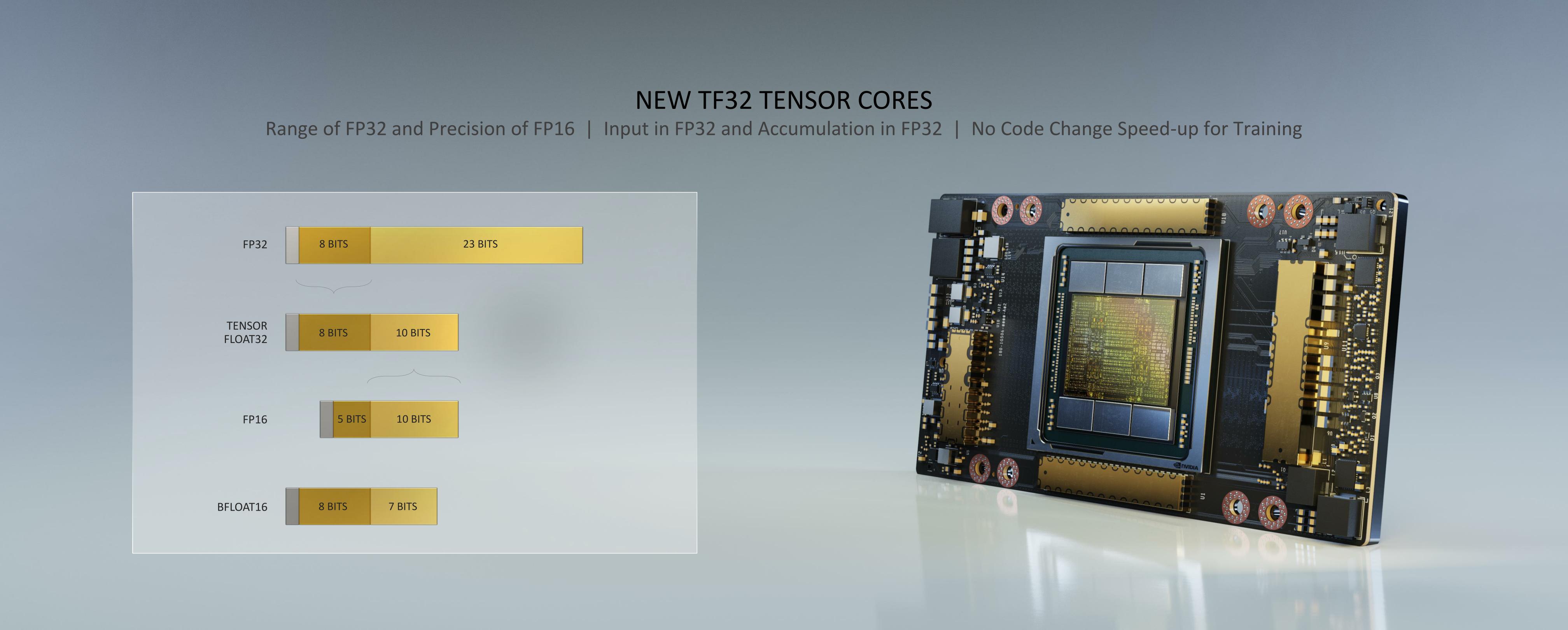
The implementation of TF32 allows NVIDIA to transparently support tensor operations on FP32 data. CUDA developers can feed the tensor cores FP32 data, where it’s internally operated on as TF32, and then accumulated and returned as FP32. The effective rate of this format is one-half the rate for pure FP16, or in the case of the A100 in particular, 156 TFLOPs. As the first part with TF32 support there’s no true analog in earlier NVIDIA accelerators, but by using the tensor cores it’s 20 times faster than doing the same math on V100’s CUDA cores. Which is one of the reasons that NVIDIA is touting the A100 as being “20x” faster than Volta.
Alternatively, developers can use bfloat16, a format popularized by Intel. The alternative 16bit format is fully supported by Ampere’s tensor cores (as well as its CUDA cores), at the same throughput as FP16. Or to take things to the extreme, NVIDIA even offers FP64 support on Ampere’s tensor cores. The throughput rate is vastly lower than FP16/TF32 – a strong hint that NVIDIA is running it over several rounds – but they can still deliver 19.5 TFLOPs of FP64 tensor throughput, which is 2x the natural FP64 rate of A100’s CUDA cores, and 2.5x the rate that the V100 could do similar matrix math.
As for inference, INT8, INT4, and INT1 tensor operations are all supported, just as they were on Turing. This means that A100 is equally capable in formats, and far faster given just how much hardware NVIDIA is throwing at tensor operations altogether.
And a lot of hardware it is. While NVIDIA’s specifications don’t easily capture this, Ampere’s updated tensor cores offer even higher throughput per core than Volta/Turing’s did. A single Ampere tensor core has 4x the FMA throughput as a Volta tensor core, which has allowed NVIDIA to halve the total number of tensor cores per SM – going from 8 cores to 4 – and still deliver a functional 2x increase in FMA throughput. In essence, a single Ampere tensor core has become an even larger massive matrix multiplication machine, and I’ll be curious to see what NVIDIA’s deep dives have to say about what that means for efficiency and keeping the tensor cores fed.
Sparsity Acceleration: Go Faster By Doing Less Work
But NVIDIA didn’t stop by just making faster tensor cores with a larger number of supported formats. New to the Ampere architecture, NVIDIA is introducing support for sparsity acceleration. And while I can’t do the subject of neural network sparsity justice in an article this short, at a high level the concept involves pruning the less useful weights out of a network, leaving behind just the most important weights. Conceptually this results in a sparse matrix of weights (and hence the term sparsity acceleration), where only half of the cells are a non-zero value. And with half of the cells pruned, the resulting neural network can be processed by A100 at effectively twice the rate. The net result then is that usiing sparsity acceleration doubles the performance of NVIDIA’s tensor cores.
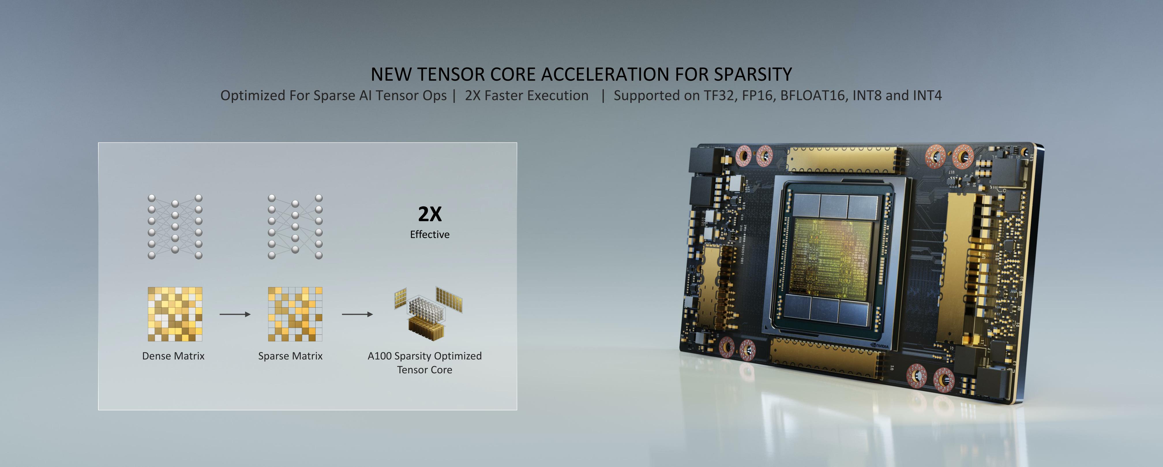
Of course, any time you talk about throwing out half of a neural network or other dataset, it raises some eyebrows, and for good reason. According to NVIDIA, the method they’ve developed using a 2:4 structured sparsity pattern results in “virtually no loss in inferencing accuracy”, with the company basing it on a multitude of different networks. None the less, sparsity is an optional feature that developers will need to specifically invoke. But when it can be safely used, it pushes the theoretical throughput of the A100 to over 1200 TOPs in the case of an INT8 inference task.
Multi-Instance GPU: Dedicated GPU Partitioning
Continuing down this tensor and AI-focused path, Ampere’s third major architectural feature is designed to help NVIDIA’s customers put the massive GPU to good use, especially in the case of inference. And that feature is Multi-Instance GPU (MIG). A mechanism for GPU partitioning, MIG allows for a single A100 to be partitioned into up to 7 virtual GPUs, each of which gets its own dedicated allocation of SMs, L2 cache, and memory controllers. The idea behind this system, as with CPU partitioning and virtualization, is to give the user/task running in each partition dedicated resources and a predictable level of performance.
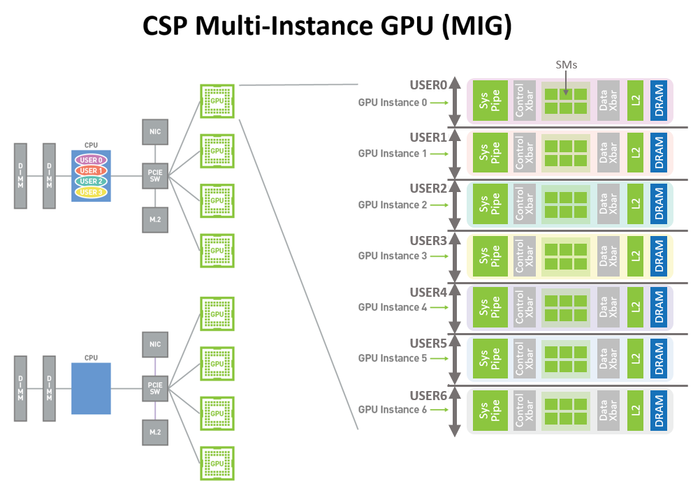
MIG follows earlier NVIDIA efforts in this field, which have offered similar partitioning for virtual graphics needs (e.g. GRID), however Volta did not have a partitioning mechanism for compute. As a result, while Volta can run jobs from multiple users on separate SMs, it cannot guarantee resource access or prevent a job from consuming the majority of the L2 cache or memory bandwidth. MIG, by comparison, gives each partition dedicated L2 cache and memory, making each slice of the GPU fully complete, and yet completely isolated.
Overall, NVIDIA says that they envision several different use cases for MIG. At a fundamental level, it’s a virtualization technology, allowing cloud operators and others to better allocate compute time on an A100. MIG instances provide hard isolation between each other – including fault tolerance – as well as the aforementioned performance predictability. From a business standpoint this will help cloud providers raise their GPU utilization rates – they no longer need to overprovision as a safety margin – packing more users on to a single GPU.
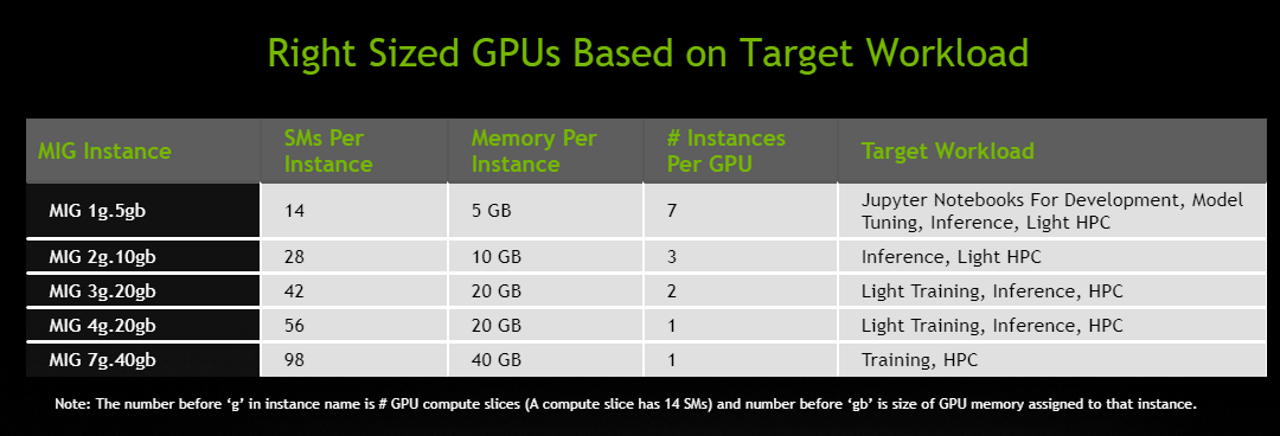
At the same time, MIG is also the answer to how one incredibly beefy A100 can be a proper replacement for several T4-type accelerators. Because many inference jobs do not require the massive amount of resources available across a complete A100, MIG is the means to subdividing an A100 into smaller chunks that are more appropriately sized for inference tasks. And thus cloud providers, hyperscalers, and others can replace boxes of T4 accelerators with a smaller number of A100 boxes, saving space and power while still being able to run numerous different compute jobs. Overall, NVIDIA is touting a minimum size A100 instance (MIG 1g) as being able to offer the performance of a single V100 accelerator; though it goes without saying that the actual performance difference will depend on the nature of the workload and how much it benefits from Ampere’s other architectural changes.
NVLink: Faster Links, Thinner Links
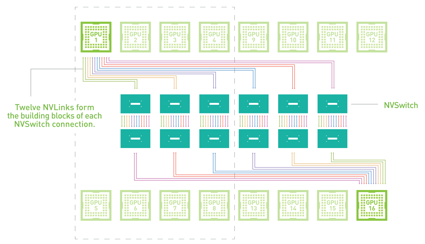
The final Ampere architectural feature that NVIDIA is focusing on today – and finally getting away from tensor workloads in particular – is the third generation of NVIDIA’s NVLink interconnect technology. First introduced in 2016 with the Pascal P100 GPU, NVLink is NVIDIA’s proprietary high bandwidth interconnect, which is designed to allow up to 16 GPUs to be connected to each other to operate as a single cluster, for larger workloads that need more performance than a single GPU can offer. For Volta, NVIDIA gave NVLink a minor revision, adding some additional links to V100 and bumping up the data rate by 25%. Meanwhile, for A100 and NVLink 3, this time around NVIDIA is undertaking a much bigger upgrade, doubling the amount of aggregate bandwidth available via NVLinks.
All told, there are two big changes to NVLink 3 compared to NVLink 2, which serve both to offer more bandwidth as well as to offer additional topology and link options. First and foremost, NVIDIA has effectively doubled the signaling rate for NVLink, going from 25.78Gbps on NVLink 2 to 50Gbps on NVLink 3. This keeps NVLink in lockstep with other interconnect technologies, many of which are similarly upgrading to faster signaling.
The other big change is that, in light of doubling the signaling rate, NVIDIA is also halving the number of signal pairs/lanes within a single NVLink, dropping from 8 pairs to 4. The net result is that the amount of bandwidth available within a single NVLink is unchanged, at 25GB/sec up and 25GB/sec down (or 50GB/sec aggregate, as is often thrown around), but it can be accomplished with half as many lanes.
| NVLink Specification Comparison | |||||
| NVLink 3 | NVLink 2 | NVLink (1) | |||
| Signaling Rate | 50 Gbps | 25 Gbps | 20 Gbps | ||
| Lanes/Link | 4 | 8 | 8 | ||
| Bandwidth/Direction/Link | 25 GB/sec | 25 GB/sec | 20 GB/sec | ||
| Total Bandwidth/Link | 50 GB/sec | 50 GB/sec | 40 GB/sec | ||
| Links/Chip | 12 (A100) |
6 (V100) |
4 (P100) |
||
| Bandwidth/Chip | 600 GB/sec | 300 GB/sec | 160 GB/sec | ||
For A100 in particular, NVIDIA has used the gains from these smaller NVLinks to double the number of NVLinks available on the GPU. So while V100 offered 6 NVLinks for a total bandwidth of 300GB/sec, A100 offers 12 NVLinks for a total bandwidth of 600GB/sec. Which at a high level sounds misleading – that NVIDIA simply added more NVLinks – but in reality the number of high speed signaling pairs hasn’t changed, only their allocation has. The real improvement in NVLink that’s driving more bandwidth is the fundamental improvement in the signaling rate.
These narrower NVLinks in turn will open up new options for NVIDIA and its customers with regards to NVLink topologies. Previously, the 6 link layout of V100 meant that an 8 GPU configuration required using a hybrid mesh cube design, where only some of the GPUs were directly connected to others. But with 12 links, it becomes possible to have an 8 GPU configuration where each and every GPU is directly connected to each other. It also offers new topology options when using NVIDIA’s NVSwitches – there NVLink data switch chips – as a single GPU can now connect to more switches. On which note, NVIDIA is also rolling out a new generation of NVSwitches to support NVLink 3’s faster signaling rate.
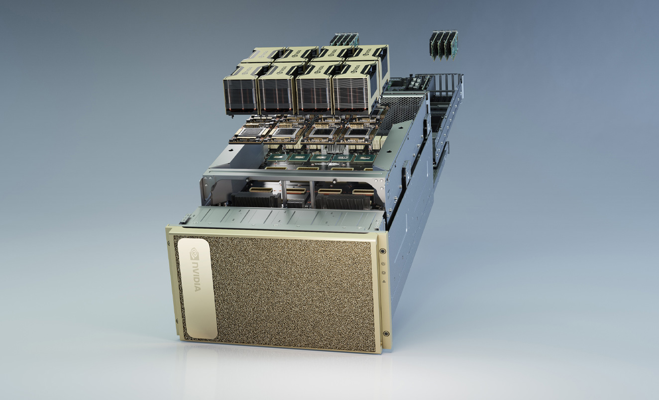
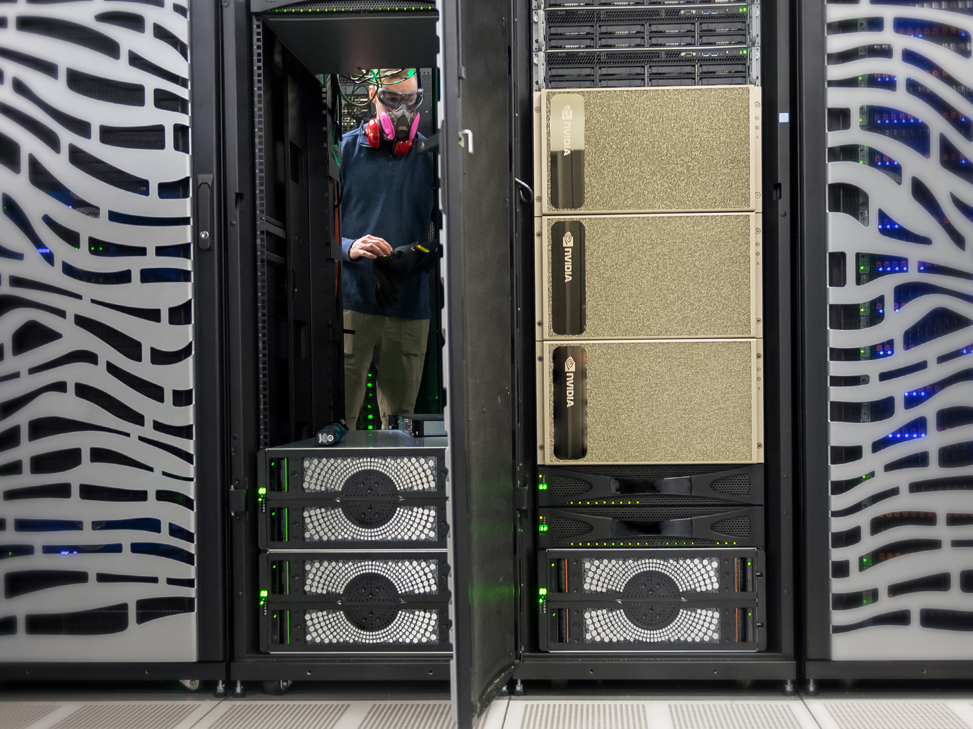
A100 Accelerator: Shipping Now in the DGX A100
Last but not least, let’s talk about when the A100 will be available. According to NVIDIA, the GPU and accelerator is already in full production, and in fact the company is already shipping their first GPUs as part of their new DGX A100 system. The latest in NVIDIA’s line of DGX servers, the DGX 100 is a complete system that incorporates 8 A100 accelerators, as well as 15 TB of storage, dual AMD Rome 7742 CPUs (64C/each), 1 TB of RAM, and HDR InfiniBand powered by Mellanox controllers. As with the Volta launch, NVIDIA is shipping A100 accelerators here first, so for the moment this is the quickest way to get an A100 accelerator.
Being among the first to get an A100 does come with a hefty price tag, however: the DGX A100 will set you back a cool $199K. Which, refrains of “the more you buy, the more you save” aside, is $50K more than what the DGX-1V was priced at back in 2017. So the price tag to be an early adopter has gone up.
In the meantime, according to NVIDIA the honor of receiving the first DGX systems has gone to Argonne National Laboratory, where the lab has already begun installing DGX A100 servers.


124 Comments
View All Comments
Farwalker2u - Friday, May 15, 2020 - link
The post of Deicidium369 you linked on imgur, specifically the highlighted portion is consistent with his post above.Deicidium369 noted he started a woodworking hobby at age 8, he stated he started with next to nothing and built up a complete workshop over a period of 40 years. That is all consistent.
I do not know whether you suffer from some form of dyslexia or what, but you seem to jumble a lot of stuff together without reason, then your version makes no sense.
Rοb - Friday, May 15, 2020 - link
He said he pays cheap, so it's probably not all BS.Gastec - Sunday, May 17, 2020 - link
Deicidium369 looks like a troll. This is what it posted further down in this comments section:"6th [stack] might be for sideband/native HBM ECC. ECC on HBM is not usually inline like on DDR"
Do you know of many millionaires and business owners to have that language or even have the time or interest to write comments on tech sites?
mode_13h - Sunday, May 17, 2020 - link
Eh, he said his businesses are idled, which is plausible. His activity on this site started about when the lockdowns hit.Many tech entrepreneurs probably started out as tech enthusiasts.
mrvco - Sunday, May 17, 2020 - link
Seek help. Seriously. Call a friend, family member or a professional.mode_13h - Sunday, May 17, 2020 - link
@Korguz, drop the fixation with his personal & business life. Please stick to commenting the technical content of his posts, or pointing out if/when he displays a lack of decorum.dersteffeneilers - Saturday, May 16, 2020 - link
ok this is epicGastec - Sunday, May 17, 2020 - link
Let me guess, you are also a programmer and if you are not yet, you could be at any moment :)Gastec - Sunday, May 17, 2020 - link
Now I've read better between the lines of Delirium369 and I can only ROFL! Good trolling but I suspect mental disturbances :)tamalero - Sunday, May 17, 2020 - link
Deicidium's post reads similar to the infamous gorilla warfare meme.