Intel’s Manufacturing Roadmap from 2019 to 2029: Back Porting, 7nm, 5nm, 3nm, 2nm, and 1.4 nm
by Dr. Ian Cutress on December 11, 2019 3:00 PM EST
Update: After some emailing back and forth, we can confirm that the slide that Intel's partner ASML presented at the IEDM conference is actually an altered version of what Intel presented for the September 2019 source. ASML added animations to the slide such that the bottom row of dates correspond to specific nodes, however at the time we didn't spot these animations (neither did it seem did the rest of the press). It should be noted that the correlation that ASML made to exact node names isn't so much a stretch of the imagination to piece together, however it has been requested that we also add the original Intel slide to provide context to what Intel is saying compared to what was presented by ASML. Some of the wording in the article has changed to reflect this. Our analysis is still relevant.
One of the interesting disclosures here at the IEEE International Electron Devices Meeting (IEDM) has been around new and upcoming process node technologies. Almost every session so far this week has covered 7nm, 5nm, and 3nm processes (as the industry calls them). What we didn’t expect to see disclosed was an extended roadmap of Intel’s upcoming manufacturing processes. It should be noted that the slide presented at the conference by Intel's partner, ASML, was modified slightly from its original source.
They say a slide is worth 1000 words. Here’s 1000 words on Intel's future.
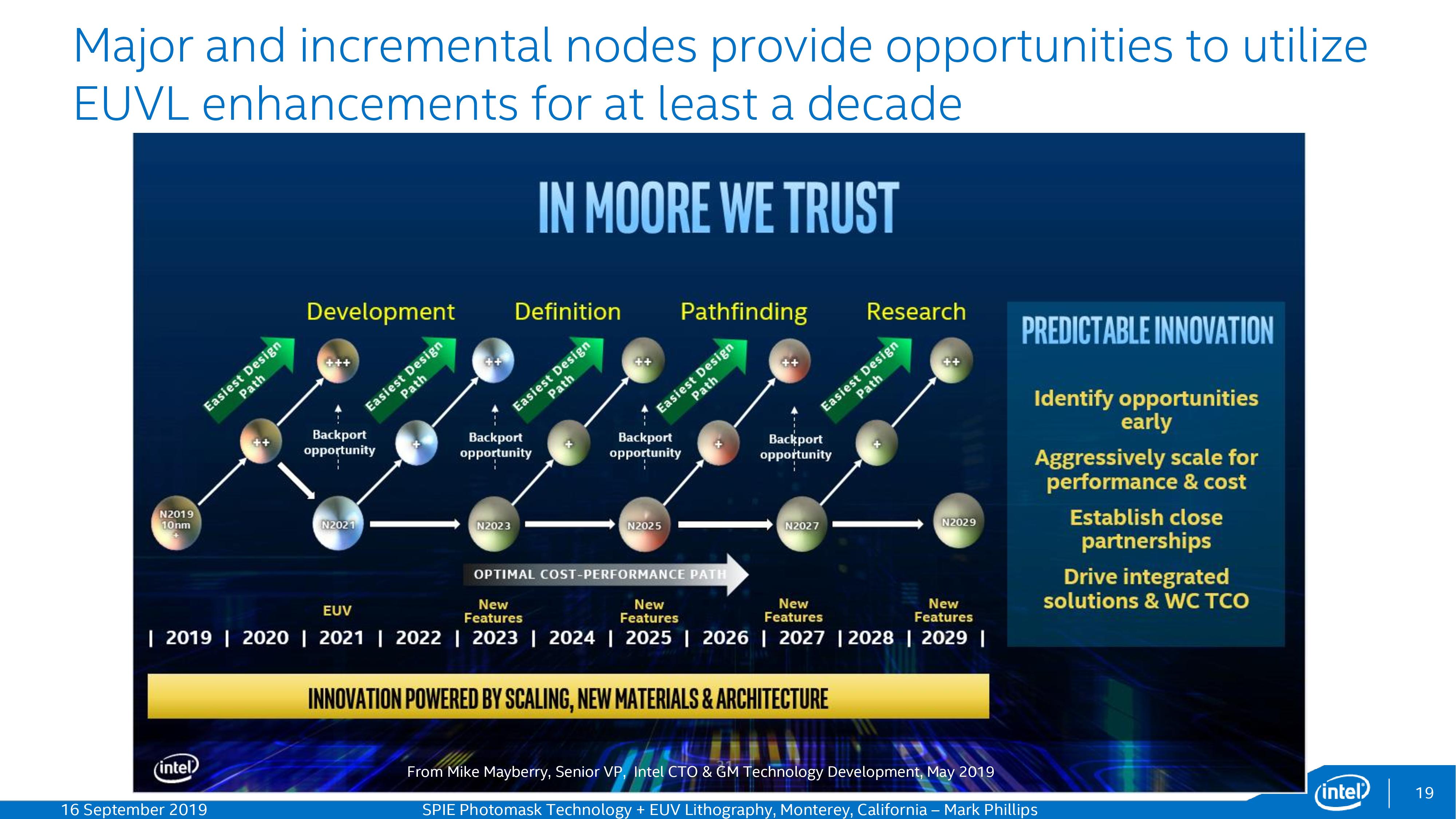
Intel's slide, as presented in September
This is Intel's original slide, not detailing which nodes in which years. However, it should be easy enough to figure out that each one of the elements in the bottom row is the next process node along, otherwise the +/++ wouldn't make sense.
ASML applied these assumptions to the slide it presented at the IEDM keynote, but the company did not disclose that they had modified the slide.
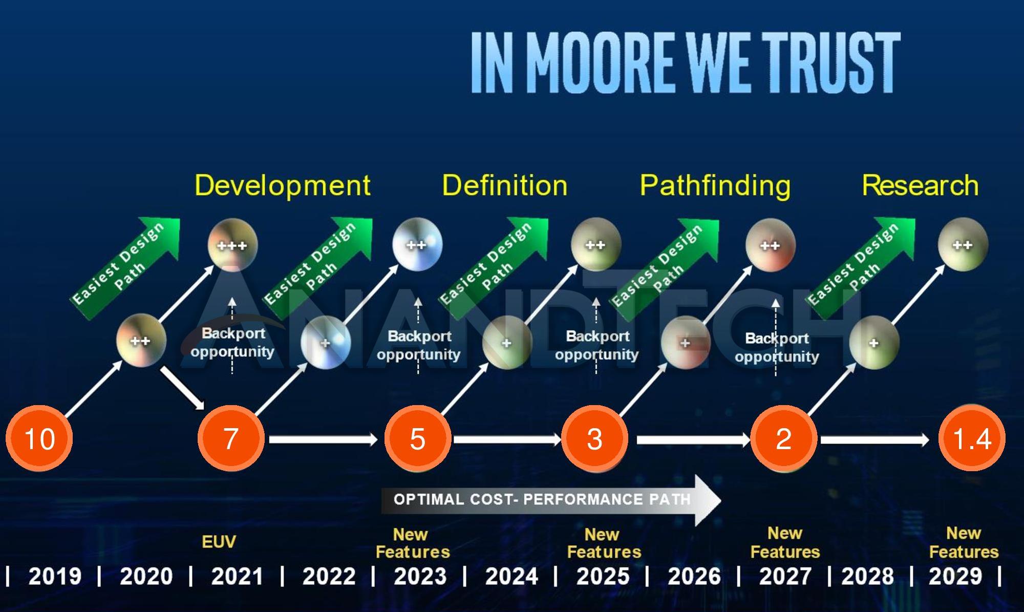
Intel's slide with ASML's animations overlayed, as shown in the slide deck distributed by ASML
So let’s go through some key areas.
1.4nm in 2029
Intel expects to be on 2 year cadence with its manufacturing process node technology, starting with 10nm in 2019 and moving to 7nm EUV in 2021, then a fundamental new node in each of 2023, 2025, 2027, 2029. This final node is what ASML has dubbed '1.4nm'. This is the first mention on 1.4nm in the context of Intel on any Intel-related slide. For context, if that 1.4nm is indicative of any actual feature, would be the equivalent of 12 silicon atoms across.
It is perhaps worth noting that some of the talks at this year’s IEDM features dimensions on the order of 0.3nm with what are called ‘2D self-assembly’ materials, so something this low isn’t unheard of, but it is unheard of in silicon. Obviously there are many issues going that small that Intel (and its partners) will have to overcome.
+, ++, and Back Porting
In between each process node, as Intel has stated before, there will be iterative + and ++ versions of each in order to extract performance from each process node. The only exception to this is 10nm, which is already on 10+, so we will see 10++ and 10+++ in 2020 and 2021 respectively. Intel believes they can do this on a yearly cadence, but also have overlapping teams to ensure that one full process node can overlap with another.
The interesting element to these slides is the mention of back porting. This is the ability for a chip to be designed with one process node in mind, but perhaps due to delays, can be remade on an older ‘++’ version of a process node in the same timeframe. Despite Intel stating that they are disaggregating chip design from process node technology, at some point there has to be a commitment to a process node in order to start the layouts in silicon. At that point the process node procedure is kind of locked, especially when it goes to mask creation.
In the slide, it shows that Intel is going to allow a workflow such that any first gen 7nm design could be back ported to 10+++, any first gen 5nm design could be back ported to 7++, and so on. One can argue that this roadmap might not be so strict with the dates – we have seen Intel’s 10nm take a long time to bake, so expecting the company to move with a yearly cadence on + updates alongside a two-year cadence with main process technology nodes would appear to be a very optimistic and aggressive cadence strategy.
Note that this isn’t the first mention of back porting hardware designs when it comes to Intel. With the current delays to Intel’s 10nm process technology, it has been widely rumoured that some of Intel’s future CPU microarchitecture designs, originally designed with 10nm (or 10+, 10++) in mind might actually find a home on a 14nm process due to the success of that process node.
Development and Research
Normally with process node developments, there will be different teams working on each process node. This slide states that Intel is currently in development of its 10+++ optimizations as well as the 7nm family. The idea is that the ‘+’ updates are capturing the low hanging fruit from a design standpoint every generation, and the number represents a full node benefit. Interestingly we see Intel’s 7nm being based on 10++, whereas in the future Intel sees 5nm come from the base 7nm design, and 3nm coming from 5nm. There is no doubt that some of the optimizations that enter each +/++ update will filter into future designs as and when they are needed.
In this slide, we have Intel’s 2023 node currently in the definition stage. At this IEDM conference there’s a lot of talk about 5nm in this timeframe, so some of those improvements (such as manufacturing, materials, consistency, etc.) will ultimately end up in Intel’s process depending on which design houses they partner with (historically Applied Materials). It is worth noting that 5nm is listed as a 2023 node, which is around the time that ASML will start selling its ‘High NA’ EUV machines to help with better path definition during the manufacturing process. I’m not sure if High NA will intercept at 5nm or 3nm, assuming this Intel roadmap has its dates correct and Intel is able to stick to it, but it is something to consider
Beyond 2023, Intel is currently in the ‘path-finding’ and 'research' mode. As always when looking this far out, Intel is considering new materials, new transistor designs, and such. At this IEDM conference we’re seeing a lot of talk of gate-all-around transistors, either as nano-sheets or nano-wires, so no doubt we’re going to see some of that as FinFET runs out of steam. TSMC is still using FinFETs for its 5nm process (Intel’s 7nm equivalent), so I wouldn’t be surprised if we see something like nano-sheets then nano-wires (or even hybrid designs) come into Intel’s manufacturing stack.
It’s worth also pointing out, based on the title of this slide, that Intel still believes in Moore’s Law. Just don’t ask how much it’ll cost.


138 Comments
View All Comments
fabmonkey - Thursday, December 12, 2019 - link
At some point, I've been told that the price will reduce from CFETs and at <3nm, VFETs, meaning that things will go vertical. If you stand every gate on its end, it solves several problems at once. Imagine a wafer covered in little cFETs like a little forest. Each one might be 20-30nm long, because of the short channel effect, but they would only take up perhaps 9-15nm^2. That would be a 10x reduction on a 3x40nm finFETschizoide - Tuesday, December 10, 2019 - link
I'll wager 1000 quatloos that 2023 has Intel on the 10nm+++++++ process with 7nm nowhere to be found.peevee - Tuesday, December 10, 2019 - link
Names are cheap to give.haukionkannel - Wednesday, December 11, 2019 - link
7nm euv is much easier to do than 10nm without euv... you really seem to not know what this is really about. Intel 10nm will be the shortest nide Intel has ever made.Most likely we see longer time 7nm and 14nm and maybe even 22nm in Intel portfolio that we will see 10nm that will meet the end of line as soon as Intel 7nm euv is ready. Intel has so much money that They can develop their 14nm++++++, 10nm++ and 7nm and 5nm at the same time. They Are not depending on each others.
name99 - Wednesday, December 11, 2019 - link
It’s not JUST EUV. Remember Intel claims that their 7nm will deliver 200MTr/mm^2A stupid promise to make given that IceLake ships at half the promised 10nm density. But that’s the promise they made, and they will (justifiably!) be mocked when they drastically miss that, as I am user they will.
TSMC isn’t promising that sort of crazy upscaling for THEIR 5nm mass EUV...
Ushio01 - Tuesday, December 10, 2019 - link
So yeah it's been over 4 1/2 years since 14nm came out and 10nm desktop chips are still nowhere in sight and they suddenly expect to make node jumps every 2 years at even smaller sizes?3nm in 2029 to me is a longshot let alone anything smaller.
nandnandnand - Tuesday, December 10, 2019 - link
Maybe lack of EUV is what screwed them. Things could speed up once they start using it.ishould - Tuesday, December 10, 2019 - link
I've heard they had a hell of a time with quad-patterning on 10nm. That and trying to get a 2.7x density increase instead of a "normal" 2xname99 - Wednesday, December 11, 2019 - link
The problems is not EUV, it is constant cluelessness.There was nothing stopping them running an EUV 10nm* line in parallel with the 10nm line. but at EVERY stage of the game they found an excuse not to do this.
Hell they could backport EUV to 10nm right now if they wanted to (cf TSMC’s 7nm+) — but, like I said, constant cluelessness.
yankeeDDL - Tuesday, December 10, 2019 - link
If they can do it, the plan looks good to me: lots of things make sense.However, can they really deliver a yearly improvement cadence and a 2-3 years development cycle, after what happened on 10nm?
And also, will the ever-increasing costs justify the developments? How much will it cost to amortize the development for 2 and 1.4nm, on silicon? What would be the cost advantage of a foundry like TSMC, on such small/expensive node, over Intel's own fab?