Analyzing Intel’s Discrete Xe-HPC Graphics Disclosure: Ponte Vecchio, Rambo Cache, and Gelato
by Dr. Ian Cutress on December 24, 2019 9:30 AM ESTPonte Vecchio: The Old Bridge in the land of Gelato
With the disclosures about Xe-HPC and the new compute unit and memory fabric in mind, Intel went onto the big money announcement: the first Xe-HPC GPU will be a design called Ponte Vecchio (PVC).
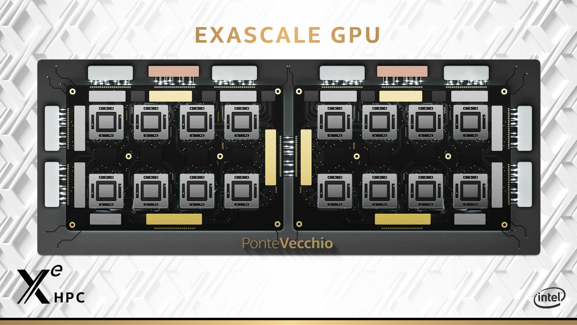
If that looks like a weird GPU to you, then I agree. What we have are two segments, each with eight compute chiplets, a number of XeMF chips, and HBM memory. I do want to step back a second to talk about some of the technologies around PVC before going into what we see here.
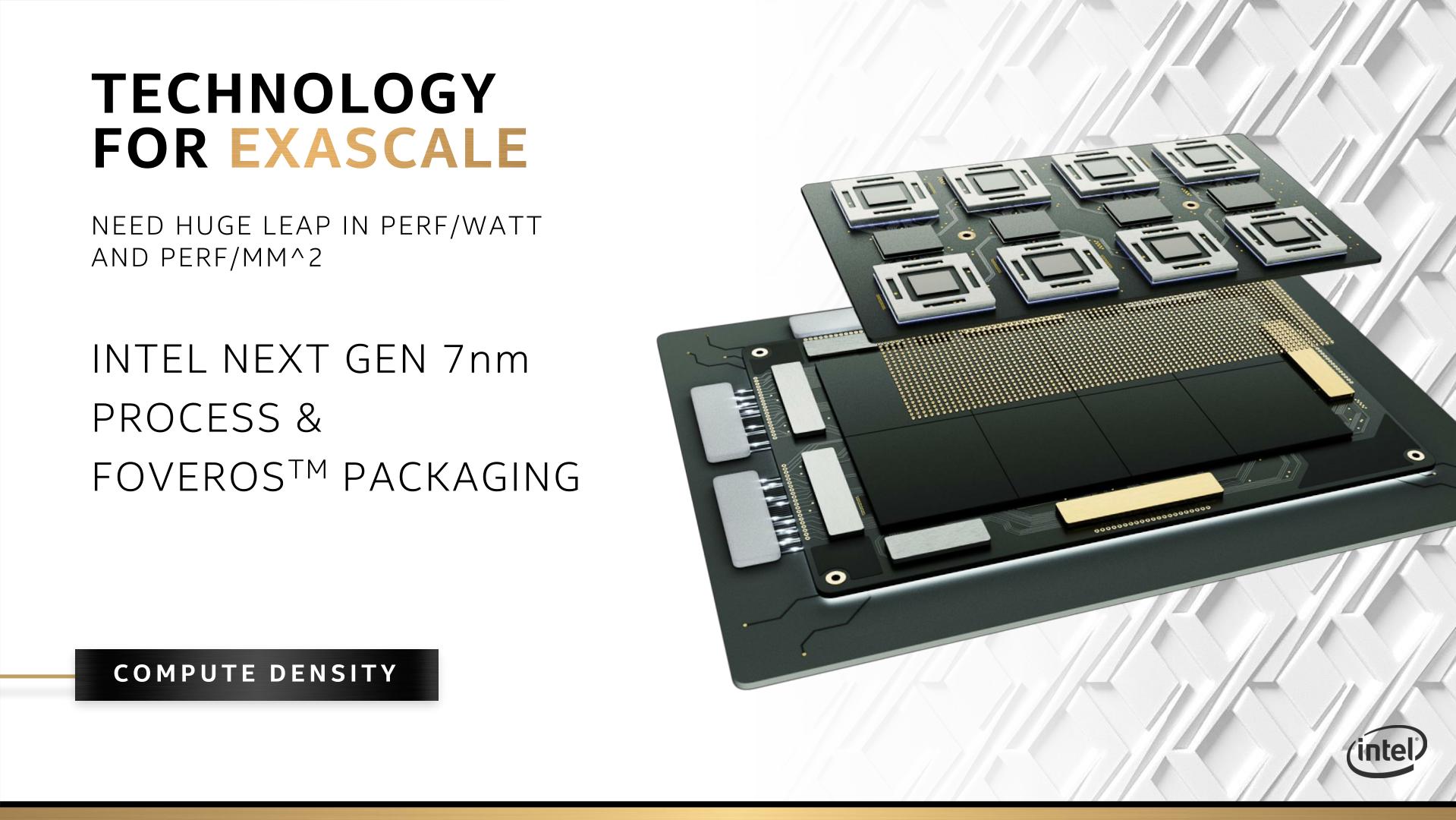
Earlier in 2019, I was offered a chance to speak to Intel’s Ramune Nagisetty. She’s in charge of Intel’s plans regarding chiplet and connectivity technologies: she’s the person to speak to when it comes to connecting chiplets with technologies like the Embedded Multi-Die Interconnect Bridge (EMIB), but also when it comes to new stacking technologies like Foveros. We’ve already seen EMIB in a number of products, such as Intel’s FPGA family, and consumer hardware like Kaby Lake-G, and Foveros is getting its first limelight in the new Lakefield chip for small-form factor client notebooks, which stacks a 14nm IO die with a 10nm Compute Die, all with a DRAM PoP on top.
In that discussion, it was confirmed what Raja had said at the Architecture Day a few months prior: both EMIB and Foveros will be coming to Intel’s new family of GPUs. Of course, EMIB and Foveros doesn’t come cheap: trying to align vias between silicon is best done when sober and with a clear head, and even then there are always optimizations to be made. In that regard, we assumed EMIB and Foveros would be going on the high-end discrete graphics solutions, what we now know to be Xe-HP. But it would appear that these technologies are likely to be in Xe-HPC as a priority, and Ponte Vecchio seems to be the first chip that will have both.
It is worth noting that technologies like EMIB and Foveros are going to define Intel’s future. Not only in GPUs, but also CPUs, FPGAs, AI, and everything else.
This slide shows that both technologies will be on Ponte Vecchio, but this slide actually says something a lot more than what it appears.
One of the questions with EMIB and Foveros is in what form it will take. There are many possibilities for both, and this slide might have exposed a few. Note that this slide only shows half of a Ponte Vecchio, and I want to do a custom diagram for you so show what I’m seeing here.
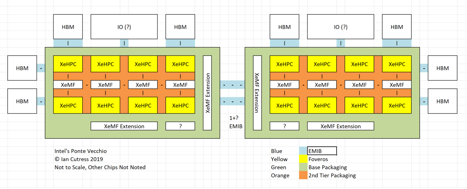
Here I’ve expanded out to a full PVC, with 16 Xe-HPC chiplets, 8 XeMF chips, and each half of the PVC has access to four HBM stacks. Each of the HBM stacks is connected via EMIB, along with what I think is an IO chip (perhaps built on 14nm).
From the official slide above, you will notice the group of 8 Xe-HPC chiplets and four XeMF chips seem to be on a separate package altogether, with a unified BGA onto another tier (the mid-tier) of packaging below. To be honest, that slide also looks like there are some chips on that mid package, but on this mid-package we also get the EMIB connections and what I believe is an XeMF scaling chip for off-GPU connections. The HBM2 and what IO chip seem to be on a bottom tier of packaging, which means that we have three tiers of packaging for this individual GPU: four if you include the Foveros on each of the Xe-HPC chiplets!
Now normally when we think of tiered packaging like this, we expect it to be BGA on BGA. There could be a part of this design that uses an interposer. If Intel was making this at TSMC, I might use the word ‘CoWoS’ as part of the stacking technology they use. At the minute it’s all a lot of guesswork. Assuming the diagram is accurate.
I’ve labelled each of the Xe-HPC chiplets as having Foveros, as we believe these to be two die stacked. A lot of commentary around this stacking is asking the question of what exactly are on each of the two dies that are stacked – is one IO and the other compute, like in Lakefield, or is it something else? A semi-reasonable conclusion is that one die might be cache, and the other die might be compute. However it’s important to note that GPUs tend to have local cache right next to the compute, to in actual fact I expect both of these dies in the Foveros stack to both be compute dies. It may be such that one is for SIMD and the other is for SIMT, but if the two were identical and modular then it makes it much easier to manufacture.
For those of you wondering what those metal brackets are around each of the Xe-HPC dies, those are likely to be shims to help correct for different chip heights. I should point out that the die inside the ship, the stacked Xe-HPC die, is actually smaller in the diagram than the XeMF die between each pair of chiplets. This could be for all the cache on the XeMF dies, or it could be if they are built on a different process node.
Also, it is worth noting that with Ponte Vecchio, we have two ‘slices’. From the diagram, it looks like that each slice has additional XeMF connection points, which could be used to go off-GPU, or so more slices (up to four) could be connected together. Some of that we might address when we look at the Aurora system and Intel’s proposed layout of one of the servers.
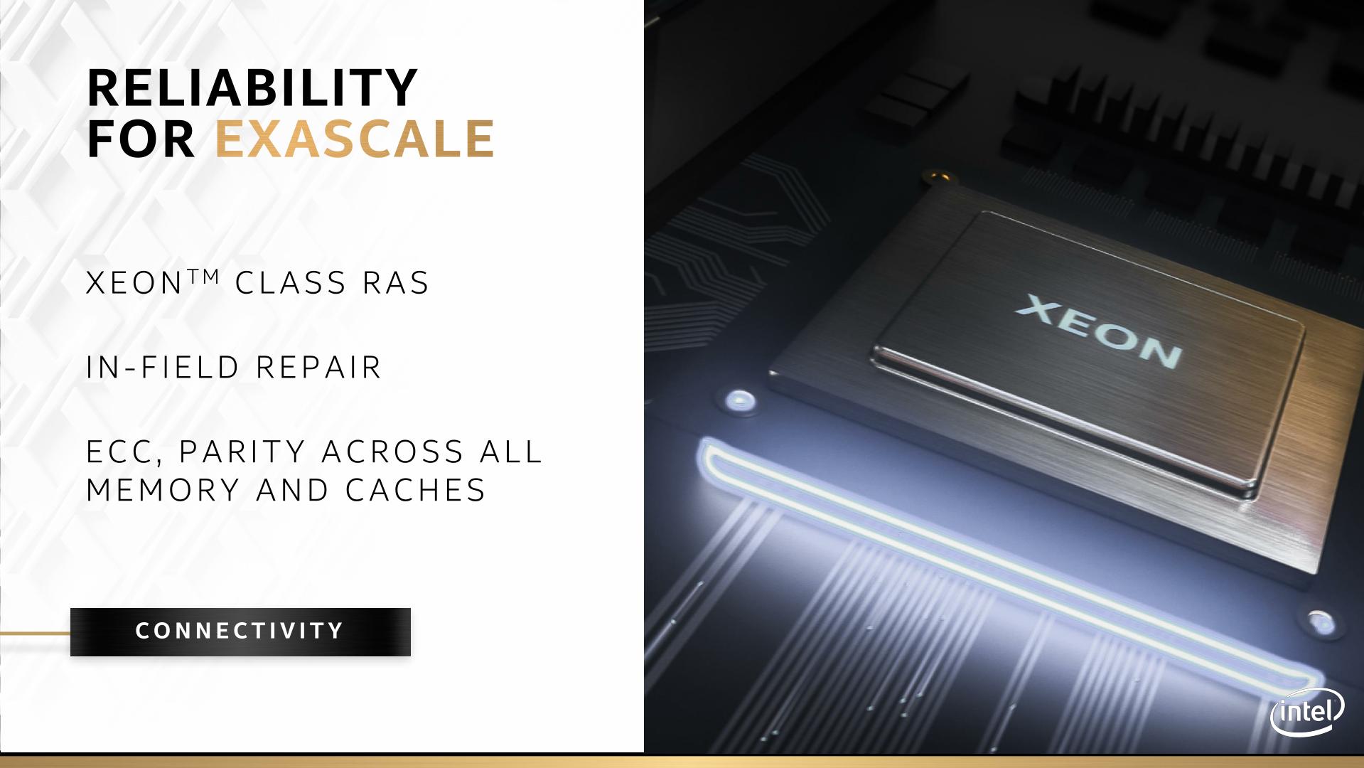
Intel promises a couple of other PVC features. Not only will the hardware support ECC and parity checks across all memory and caches, but there will be Xeon-class RAS features and something called ‘in-field repair’. More details to come.
Also, a final word on the name: Ponte Vecchio. Intel has plenty of Lakes, Coves, Rapids, and other things. Apparently having a codename that involves a physical place actually helps address any potential legal issues without having to do due diligence for a proper marketing name. Raja Koduri said that he chose it because it’s based in Florence, which has good gelato. He likes gelato, and should Intel decide to do a launch event with Ponte Vecchio in mind, Raja gets his gelato. I went to Florence a couple of years ago – the gelato was good.


47 Comments
View All Comments
martinw - Tuesday, December 24, 2019 - link
> we’re looking at 66.6 TeraFLOPs per GPU. Current GPUs will do in the region of 14 TF on FP32, so we could assume that Intel is looking at a ~5x increase in per-GPU performance by 2021/2022 for HPC.But HPC ExaFLOPs are traditionally measured using FP64, so that means a ~10x increase.
Santoval - Tuesday, December 24, 2019 - link
If Intel manage to deliver ~67 TFLOPs of *double* precision in a single GPU package -even if it consists of multiple GPU chiplets- I will eat the hat I don't have. ~67 TFLOPs of single precision in a single GPU package might be possible (at a 480 - 500W TDP) due to Intel's new GPU design and its 7nm node, which should be quite more power efficient than their 10nm & 14nm nodes, assuming Intel can fab it at a tolerable yield that is.The use of Foveros and EMIB also reduce the power budget and increase performance further, because they alleviate I/O power draw and, along with that "Rambo cache", mitigate the memory bottleneck. The graphics memory will also probably be HBM3, with quite a higher performance and energy efficiency.
So a ~5x performance at roughly x2 the TDP of the RTX 2080 Ti might be doable. It is ~2.5 times the performance per watt, which is high but not excessive. To double that performance further though is impossible. Intel are a semiconductor company, they are not wizards.
nft76 - Wednesday, December 25, 2019 - link
I'm guessing the number of nodes (and GPUs) will be at least two, probably more like three to four times larger than estimated in the article. I'm guessing that the ~200 racks is without storage included and there will be more nodes per rack. If I'm not mistaken, Cray Shasta high-density racks are much larger than standard.eastcoast_pete - Tuesday, December 24, 2019 - link
Thanks Ian, Happy Holidays to All at AT and here in "Comments"!My first thought was, boy, that lower case/upper case in oneAPI is really necessary; reading the subheading, I almost thought it's about an unusual Irish name (O'NEAPI), w/o the apostrophe.
On a more serious note, this also shows how important the programming ecosystem is; IMO, a key reason why NVIDIA remains the market leader in graphics and HPC.
UltraWide - Tuesday, December 24, 2019 - link
Nvidia recognized this more than 10 years ago, everyone else is playing catch up.JayNor - Tuesday, December 24, 2019 - link
Intel is extending Sycl for FPGA config using data flow pipes. They've mentioned previously that Agilex will have the first implementation of pcie5 and CXL. Perhaps OneAPI will do something to simplify FPGA design.https://github.com/intel/llvm/blob/sycl/sycl/doc/e...
JayNor - Tuesday, December 24, 2019 - link
Intel's current NNP chips don't have PCIE5 or CXL, and I recall some discussion about it being a feature that the NNP-I chips did manual memory management.Is Intel enthusiastically pushing shared memory for the GPU high performance programming, or is this just a convenience during development to get CPU solutions working on GPU quickly?
ksec - Tuesday, December 24, 2019 - link
>The promise with Xe-HPC is a 40x increate in FP64 compute performance.Increase
One or two other spelling mistakes but I can no longer find it.
>The CPUs will be Sapphire Rapids CPUs, Intel’s second generation of 10nm server processors coming after the Ice Lake Xeons
First time I heard SR will be an 10nm++ CPU, always thought it was destined for 7nm. Possibly Another Roadmap shift.
Other than that Great Article. But as with anything Recent Intel, I will believe it when I see it. They are ( intentionally or not ) leaking lots of benchmarks and roadmaps, and lots more "communication" on the ( far ) future as some sort of distraction against AMD.
I have my doubt on their GPU Drivers, not entirely sure their 10nm yield and cost could compete against NV and AMD without lowering margin. But at least in terms of GPGPU it will bring some competition to Nvidia's ridiculously expensive solution.
Alexvrb - Tuesday, December 24, 2019 - link
Yeah they'll probably be more competitive in HPC in the short term. For gaming... we'll see. I suspect they'll get murdered in the short term unless they are really aggressive with pricing. If they go this route most likely they'll do CPU+GPU bundle deals with OEMs to force their way into the "gaming" market.Spunjji - Friday, December 27, 2019 - link
That approach seems highly likely.