The Huawei Mate 30 Pro Review: Top Hardware without Google?
by Andrei Frumusanu on November 27, 2019 10:00 AM EST- Posted in
- Mobile
- Smartphones
- Huawei
- Kirin 990
- Mate 30 Pro
The Kirin 990 SoC
The Kirin 990 is an unusual SoC this year for the fact that there’s two variants of the chip. Huawei and HiSilicon have opted to hedge their bets in terms of silicon manufacturing with TSMC and create two versions of the chipset: The regular 4G variant is created using the existing TSMC N7 manufacturing process which was also used for the previous generation Kirin 980 processor, whilst the 5G variant of the Kirin 990 is a completely altogether different chip using TSMC’s new N7+ manufacturing node which uses EUV lithography.
| Huawei Kirin 990 Family | ||||
| AnandTech | Kirin 990 5G |
Kirin 990 (4G) |
Kirin 980 | Kirin 970 |
| CPU | 2xA76 @2.86G 2xA76 @2.36G 4xA55 @1.95G |
2xA76 @2.86G 2xA76 @2.09G 4xA55 @1.86G |
2xA76 @2.60G 2xA76 @1.92G 4xA55 @1.80G |
4xA73 @2.36G 4xA53 @1.80G |
| GPU | G76MP16 600MHz |
G76MP16 600 MHz |
G76MP10 720 MHz |
G72MP12 850 MHz |
| NPU | 2 + 1 Da Vinci |
1 + 1 Da Vinci |
2 Cambricon |
1 Cambricon |
| Modem | Balong 5G | 4G | 4G | 4G |
| DRAM | LPDDR4-4266 + LLC |
LPDDR4-4266 + LLC |
LPDDR4X-4266 | LPDDR4X-3733 |
| Die Size | 113.31 mm2 | ~90 mm2 | 74.13 mm2 | 96.72 mm2 |
| Transistors | 10.3b | ~8.0b | 6.9b | 5.5b |
| Mfc. Process | N7+ | N7 | N7 | 10FF |
Although the two chipsets are two different pieces of silicon, going as far as needed different physical designs due to rule incompatibility between the N7 and N7+ nodes, the two chipsets still essentially share a lot of common features and are very similar to each other in terms of the IP they use.
Both chips follow a 2+2+4 CPU cluster setup, with two high performance A76 cores clocking in at 2.86GHz, two mid-performance cores clocking in at 2.09GHz on the 4G variant and 2.36GHz on the 5G variant, and four Cortex A55 cores at 1.86GHz for 4G and 1.95GHz for the 5G chipset. HiSilicon continues to employ a 4MB L3 cache in for the cluster.
On the GPU side, the chip uses a very large implementation of the Mali G76. At 16 cores, it’s the largest configuration of this GPU we’ve seen, and is clocked in at 600MHz.
Another auxiliary IP difference between the two variants is the fact that the 5G version employs a stronger NPU. We find a dual-core variant of the new DaVinci microarchitecture, while the 4G chipset makes due with a single core version of the IP.
Naturally, the single biggest difference between the 4G and 5G variants is implied in the names of the parts: The 5G variant comes with an additional 5G modem that isn’t found in the 4G version.

Die shot source: TechInsights - Labelling & Custom contrast: AnandTech
TechInsights has published the die shot of the new Kirin 990 5G and we took a closer look at the IP blocks that we can identify. Unfortunately, while there isn’t a public die shot of the Kirin 990 4G out there, we did have a chance to have a look at it and cross-compare the differences to the 5G version in order to better pin-point blocks such as the NPU and modem.
The Kirin 990 5G comes in at 113.31mm² which isn’t actually too big considering that HiSilicon is dedicating a lot of area to the massive GPU as well as the bigger NPU this generation. The CPU cluster at the middle of the SoC is self-explanatory and we’re able to identify the A76 as well as A55 cores. It’s interesting to see that the approach of using the same CPU IP for the “big” and “middle” cores in fact doesn’t really result in much of a physical size difference between the two groups – the biggest differences here are purely in the transistor-level implementation. This comes in contrast to Qualcomm’s 1+3 CPU configuration where the one performance cores is actually larger than the remaining three cores, partly due to the doubled L2 cache.
The DaVinci NPU would have been hard to identify weren’t it for the fact that we saw similar block structures on the 4G and 5G variants- with the difference that the 5G variant has two identical adjacent blocks while the 4G variant only has one. It’s a quite sizeable piece of the SoC so it does show that the company puts a lot of investment into AI.
The modem was the trickiest part to identify – the highlighted labelling and blocks in the image above is just my best estimate of what’s seen on the SoC. The 4G variant of the SoC completely lacks the block labelled as the 5G modem, so just by pure elimination of other possibilities we have to come to the conclusion that this is indeed the modem IP. The block is roughly a little over 15mm² in size, which while sizeable in terms of a SoC block, isn’t all that big in the grand scheme of things, especially when compared to discrete modem sizes in excess of 50-60mm².
The oddity here is that I still believe that there’s two modem subsystems and that the 4G modem as presented on the 4G Kirin 990 is still present on the 5G variant. While relocated in position, the marked group of IP must be the 4G modem IP as there’s no other difference between the 4 and 5G variants of the chip; the 5G variant merely adds in more IP blocks rathe than changing things around too much. The only major lackings on the 5G version is that I’m identifying far less interface I/O to what I believe are PCIe PHYs. Possibly because this variant of the chip has a 5G modem integrated, there’s no practical need for these additional lanes.
Finally, a big important addition to the Kirin 990 is the adoption of a new last level cache, or how we like to call it, a system level cache. The block can be identified at the centre of the chip and judging by the physical size, is 3-4MB large. HiSilicon this year is said to have paid a lot of attention to the memory subsystem and improved is performance quite a lot.
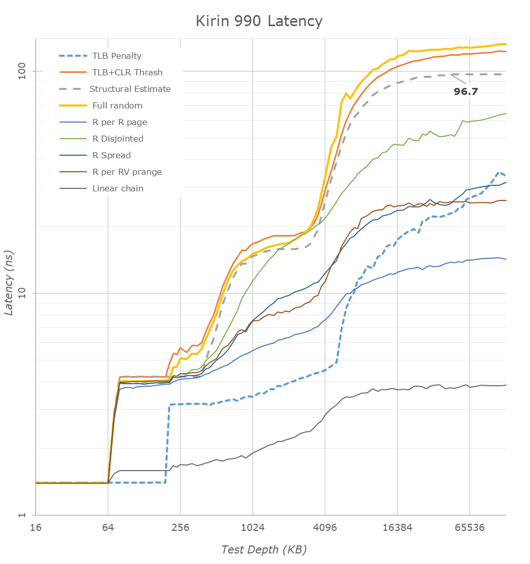
If we look at the memory latency results of the CPU, we indeed see that the company has been able shave off ~10ns of latency and achieve sub-100ns memory latency, making the new chip the fastest (Along with the Exynos 9820) in this regard, although Apple’s large caches are a different beast altogether.
It’s to be noted that we don’t see the SLC cache in the CPU’s memory latency results, evidently HiSilicon is bypassing the cache on the high-performance CPUs in order to get better latency to DRAM. We weren’t able to confirm if the middle or little cores have access to the SLC – I imagine they do as that’s also how Samsung and Qualcomm have implemented their power management policies for their SLCs.
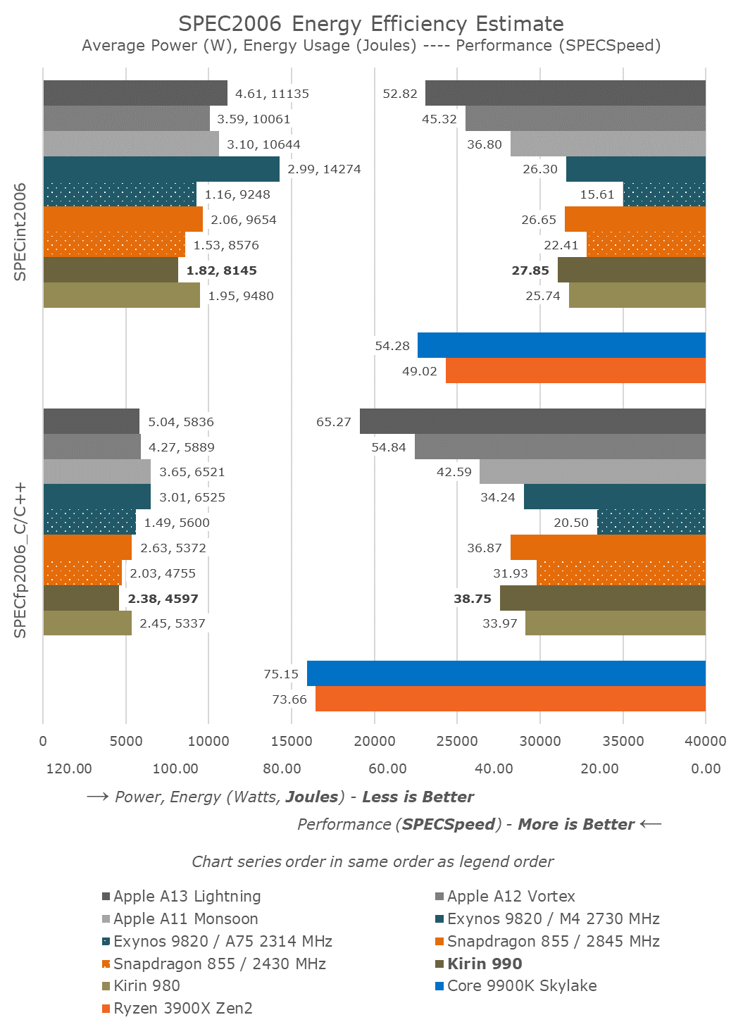
Given that the SoC doesn’t contain any new IP, we’ll spare the readers the effort of going into detailed SPEC results. However, the overview is still interesting to look at in terms of the results. As a reminder, this is the 4G variant of the Kirin 990 which uses the same manufacturing node as the Kirin 980, as well as the same CPU IP. The differences between the two chips is the improved physical design that HiSilicon was able to implement, as well as differences of the new memory subsystem.
The overall improvements here are quite impressive – the new chip sports higher performance all whilst using less energy and power. The interesting thing here is that most of these improvements in efficiency aren’t due to the better CPU implementation; there’s definitely improvements here, but they are vastly overshadowed by the improvements we’re seeing in the memory subsystem. Benchmarks which have little memory pressure and thus mostly reside on the CPU caches have the smallest improvements in terms of energy efficiency, whilst the big memory heavy benchmarks such as 429.mcf or 462.libquantum are seeing perf/W improvements of up to 27% due to both very large performance improvements as well as actual lower power usage.
So whilst HiSilicon wasn’t able to implement the new Cortex A77 CPU IP this year into the Kirin 990, the new chip shouldn’t be mistaken as simply having the same or similar performance to the Kirin 980 or Snapdragon 855 just because they have the same A76 CPU IP. The new chip is definitely faster and more efficient than the predecessors.


58 Comments
View All Comments
PenGunn - Wednesday, November 27, 2019 - link
My Mate 20 is flawless. Got a seriously good deal from Virgin in BC Canada and its the best phone I've ever had. My previous phone, a P10 was the best, until I picked up the Mate 20. All the Google crap is there. Still sideloading is easy.dudedud - Wednesday, November 27, 2019 - link
So... what's the point of the bigger NPU? It's actually used anywhere? Or at least have an advantage over the one on the 980?Kangal - Thursday, November 28, 2019 - link
The biggest advantage of the NPU is for......OEMs to say look we have Neural Link and AI-capabilities, despite not doing anything :D
s.yu - Thursday, November 28, 2019 - link
Bragging rights.cfenton - Wednesday, November 27, 2019 - link
Without side-loading APKs or installing Google Play Services, what's available on the device? Is the Huawei app store any good, or is it like Samsung's store (most of the big stuff, but nowhere near everything)?Kangal - Thursday, November 28, 2019 - link
Why has no-one else asked this question?!?(I'd think it's significantly worse than GalaxyApps, Amazon Appstore, APKpure, Aptoide and F-Droid)
cfenton - Thursday, November 28, 2019 - link
I suspect you're right, but I'd like to know for sure. I think a casual user could get away with the Amazon Appstore, and maybe even the Galaxy Store, but not anything less than that. I'd like to know, for example, how many of the top 50 apps on the Play Store are available on the Huawei store.yetanotherhuman - Thursday, November 28, 2019 - link
New SD card type. Ugh. Who do they think they are, Sony? MicroSD is small enough. It works. They're cheap, and everywhere, up to unbelievably large sizes. Let's not mess with it.s.yu - Thursday, November 28, 2019 - link
Oh they think they're Apple alright.Jostian - Thursday, November 28, 2019 - link
why only ever compare the Mate 30 P to the P30 P?? how does it compare to the iPhone 11 or Pixel etc. you have all the photos but then only compare the 2 Huawei's?? iPhone has more smearing especially in foliage and fine detail imho but really hoped the review would go beyond just the 2 Huawei's in terms of camera comparison...