Intel Cascade Lake Xeon W-3200 Launched: Server Socket, 64 PCIe 3.0 lanes
by Dr. Ian Cutress on June 10, 2019 8:00 AM EST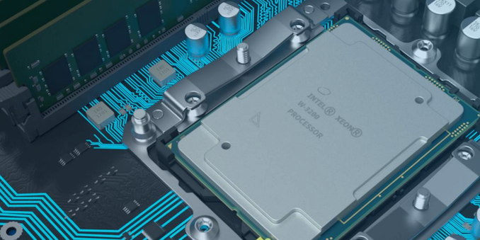
One of the quiet announcements that came out of Apple’s new Mac Pro announcement was the launch of Intel’s next generation Xeon W processors. Aside from being completely under the radar from a formal announcement, the new line of workstation focused CPUs heralds a few quirks: they are Cascade Lake based, they are only in the LGA3647 socket, and they have 64 available PCIe 3.0 lanes.
The current Xeon W product line, based on Skylake-SP, uses the common high-end desktop socket LGA2066, but with a workstation focused chipset. These processors are available up to eighteen cores, using Intel’s HCC 18-core die as the highest it will go. The other features of these processors include quad channel memory, 512GB ECC support, and up to 48 PCIe 3.0 lanes. What Intel has done for the next generation has bump it up to the server socket, which affords more memory channels, higher TDPs, more memory supported, and a higher core count.
The new Cascade Lake-based Xeon W-3200 family will be offered up to 28 cores, using Intel’s XCC 28-core die as the base for the high-end models. As a Cascade Lake processor, the new Xeon W will come with additional in-hardware fixes for some of the Spectre and Meltdown vulnerabilities, similar to the Cascade Lake Xeon Scalable Processors. Intel has also made a substantial change in the way that it intends to market its Xeon W processors, as the new models also change socket compared to the previous generation.
Historically we are afforded multiple generations of workstation CPU on the same socket, however at this time Intel has decided to forgo this application and move Xeon W from the LGA2066 socket to the LGA3647 socket, limiting users who wish to upgrade from their Xeon W-2100 processors. The new socket, combined with the new silicon, means that Intel can offer new Xeon W owners more features, although much to the chagrin of previous Xeon W owners. This doesn't exclude Intel launching another set of CPUs on the LGA2066 socket for upgrades, however given the lack of fanfare for this launch, it wouldn't seem likely that Intel has plans to do so.
The LGA3647 socket has been used in Xeon Scalable processors since Skylake-SP launch, and affords six full DDR4 memory channels. The silicon inside the new Xeon W does have six memory controllers, allowing it to take full use of this feature. (Technically the previous generation also had six memory controllers in the silicon, but the platform was limited to four, as per Intel’s product positioning strategy.)
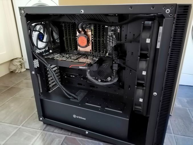
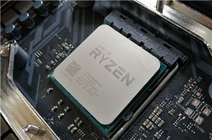
The LGA3647 system Intel sent with the last Xeon W Review Unit
As with the previous Xeon W, the cores are arranged in a block, and inside is a ‘Mesh’ which we’ve described in detail in previous reviews. One of the additional features for the Xeon W-3200 is the upgrade to a full 64 PCIe 3.0 lanes available for PCIe slots, up from the previous 48. This also makes Intel’s new Cascade Lake W-3200 family the x86 product that Intel offers with the most PCIe lanes.
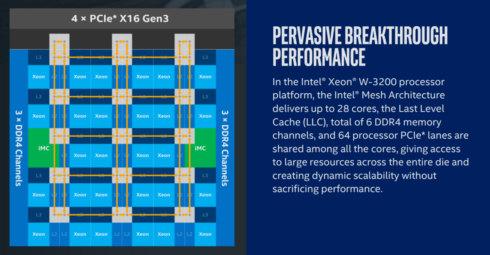
This is a bit of a technicality – previous Xeon SP and Xeon W did actually have 64 lanes on the silicon, however 16 of them were reserved for on-package chips, such as OmniPath. What Intel has done here is re-route them through the socket pins instead, allowing motherboard manufacturers to design a full x16/x16/x16/x16 layout or variants therein. This also means that the LGA3647 socket already had pins ready to be allocated to these PCIe lanes, so it would not have surprised me if Intel has already sold 64 PCIe lane custom versions to customers since the original Skylake-SP launch.

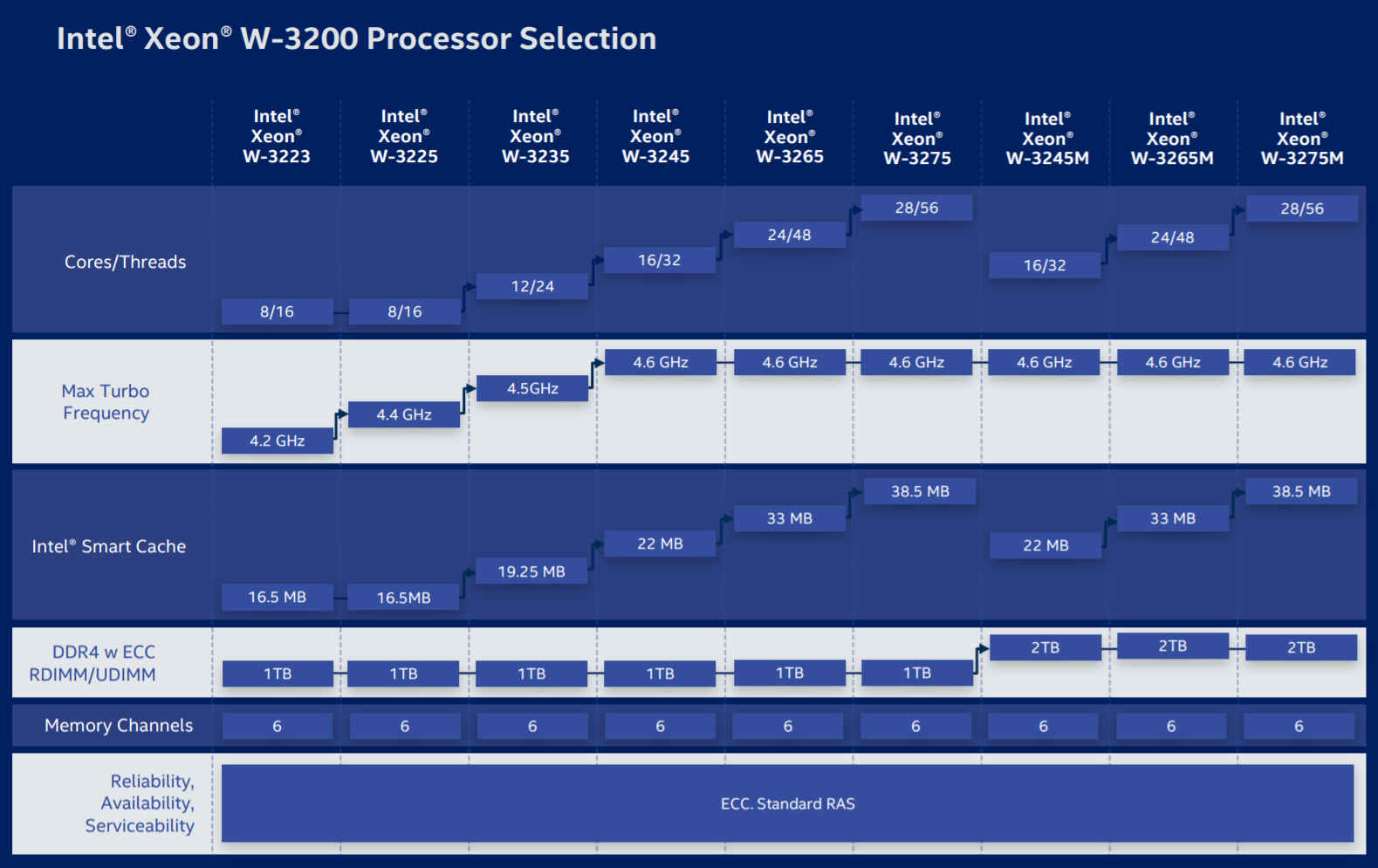
Here are the nine new CPUs:
| Intel Cascade Lake Xeon W-3200 Family | |||||||
| AnandTech | Cores Threads |
TDP | Base Freq |
Turbo 2.0 |
Turbo 3.0 |
DRAM | Price |
| W-3275M | 28C / 56T | 205 W | 2.5 GHz | 4.4 GHz | 4.6 GHz | 2 TiB | $7453 |
| W-3275 | 28C / 56T | 205 W | 2.5 GHz | 4.4 GHz | 4.6 GHz | 1 TiB | $4449 |
| W-3265M | 24C / 48T | 205 W | 2.7 GHz | 4.4 GHz | 4.6 GHz | 2 TiB | $6353 |
| W-3265 | 24C / 48T | 205 W | 2.7 GHz | 4.4 GHz | 4.6 GHz | 1 TiB | $3349 |
| W-3245M | 16C / 32T | 205 W | 3.2 GHz | 4.4 GHz | 4.6 GHz | 2 TiB | $5002 |
| W-3245 | 16C / 32T | 205 W | 3.2 GHz | 4.4 GHz | 4.6 GHz | 1 TiB | $1999 |
| W-3235 | 12C / 24T | 180 W | 3.3 GHz | 4.4 GHz | 4.5 GHz | 1 TiB | $1398 |
| W-3225 | 8C / 16T | 160 W | 3.7 GHz | 4.3 GHz | 4.4 GHz | 1 TiB | $1199 |
| W-3223 | 8C / 16T | 160 W | 3.5 GHz | 4.0 GHz | 4.2 GHz | 1 TiB | $749 |
Each CPU also supports AVX512, with two FMA units across every model. Memory support for all CPUs is listed as six channels of DDR4-2933 (except the 8 core parts , which are DDR4-2666), with a base support of 1 TiB of memory which rises to 2 TiB for the higher memory models (for an additional $3000). This also marks the first instance in which Intel is offering higher memory support SKUs for Xeon W, although it should be noted that Intel seems relatively happy these days to allow support of unbalanced memory configurations. E.g. 1 TiB split between 12 memory slots means 8 x 64GiB + 4 x 128 GiB module arrangements, or 2 TiB means 8 x 128 GiB + 4 x 256 GiB.
Another feature making its way onto these CPUs is Turbo Boost Max 3.0, which is an additional turbo setting on each CPU if the situation allows it. It should be pointed out that in-line with other workstation CPUs, these models are only built for single socket systems.
One interesting feature missing from these CPUs is Optane DC Persistent Memory support. Intel had stated at its Investor Day presentations that Optane DC Persistent Memory support was coming to the workstation processor line by the end of the year. This means that either Intel is planning another Xeon W update between now and Q1 2020, or this feature may be BIOS enabled later in its lifecycle. The other alternative is that Intel will offer Optane capable custom SKUs for specific customers.
Intel’s new Cascade Lake Xeon W processor line is currently available in the new Apple Mac Pro. We expect it to filter down into other platforms over the next two quarters, and perhaps become more widely available at retail.
| Want to keep up to date with all of our Computex 2019 Coverage? | ||||||
 Laptops |
 Hardware |
 Chips |
||||
| Follow AnandTech's breaking news here! | ||||||


56 Comments
View All Comments
Kevin G - Tuesday, June 11, 2019 - link
AMD hasn't released anything on specific models: just indicated that they'll go up to 64 cores. How they do the lesser parts is speculative and well, AMD has LOTS of options. I would fathom that they'll lower the number of cores per CCX to maximize cache usage where possible.What would be nice would be a server motherboard that would identify what chiller and CCX a core is found plus the ability to selectively disable it. Take a 33 core part and off hand there are three main ways of doing it: 8 chipslet each with one CCX disabled, 8 chiplets with two cores in each CCX disabled and then just four fully functional chiplets. I wouldn't expect large performance differences and they may only appear under certain workloads. Good research project for those doing a deep dive into the design.
Regardless, AMD has lots of options and I'm pretty sure they can use every chiplet manufactured in some fashion except to total duds. Very cost effective from a manufacturing standpoint.
techguymaxc - Monday, June 10, 2019 - link
The beauty of computers is that they can be used to run just about any workload one can dream up. For many customers, this necessitates virtualization. Most virtual workloads are memory-constrained rather than CPU. If you need to host databases, multiple environments (dev/test) you're going to need a lot of RAM.jamescox - Monday, June 10, 2019 - link
The full 8 chiplet Epyc 2 will have 256 MB of on package L3 cache. The largest intel goes up to right now is 38.5. The massive cache will reduce the load on the memory controllers significantly. Intel cannot compete with that amount of cache with 14 nm parts.MattZN - Monday, June 10, 2019 - link
That is a mind-boggling amount of L3 cache. Even the 'consumer' Ryzen chips have mind-boggling amounts of L3. The 12-core will have two chiplets... 64MB of L3.-Matt
PVG - Monday, June 10, 2019 - link
But the new Apple Mac Pro is NOT currently available...melgross - Monday, June 10, 2019 - link
Yes, Apple just announced it will be September. But as far as I know, it’s the first announced system to use this, and likely the first to ship. So we’re possibly talking 2.5 months, or so.niva - Monday, June 10, 2019 - link
Dear AnandTech, why is your website inundated with ads? We understand having some ads, but now one must scroll multiple pages down before they can get to the comments. It's getting ridiculous. Please consider the user experience. I've been a reader since 2001 and while I still love your detailed reviews the website is definitely frustrating now.alpha754293 - Monday, June 10, 2019 - link
"The current Xeon W product line, based on Skylake-SP..."Sorry, but that's incorrect.
The current Xeon W product line is based on Skylake-W. (Source: https://en.wikipedia.org/wiki/List_of_Intel_Xeon_m...
The difference between Skylake-W and Skylake-SP is that Skylake-W only supports upto 8 DIMMs of memory, for a maximum of 512 GB while the Skylake-SP supports upto 12 DIMMs of memory, for upto 768 GB for non-M SKUs and 1536 GB for M SKUs.
You cannot run Skylake-W in any other configuration besides a single socket configuration whereas Skylake-SP is for dual socket systems and up (although I suppose that in theory, you might and should still be able to run Skylake-SP in a single socket configuration, if you so desire, but I don't know if that's necessarily 100% true).
However, both Skylake-W and Skylane-SP have a maximum of 48 PCIe 3.0 lanes.
Kevin G - Monday, June 10, 2019 - link
LGA 2066 Xeon W is indeed based upon Sky Lake-SP. Intel simply changed the packaging where two of the memory channels simply are not present on LGA 2066 vs the bigger LGA 3647. Intel was rather clever here since LGA 3647 also have several on package options. Take a look at a delidded LGA 2066 part:https://www.gamersnexus.net/news-pc/2943-intel-i9-...
Notice that there is one PCB on top of another? Now take a look at a deluded LGA 3647 part:
https://www.overclock3d.net/news/cpu_mainboard/pro...
Notice the same that it is the same PCB on PCB style setup? The lower PCB dictates the socket and any on-package extras where as the upper one houses the CPU.
Similarly, the Sky Lake-SP dies have always had 64 PCIe lanes but if them never made it to the motherboard: there were for Omnipath or FPGA options in the package.
ZoZo - Monday, June 10, 2019 - link
It would have been nice to have a W-3235X or W-3245XOr if they could add ECC support to the HEDT platform, that would do the trick for me too.