Intel's Architecture Day 2018: The Future of Core, Intel GPUs, 10nm, and Hybrid x86
by Dr. Ian Cutress on December 12, 2018 9:00 AM EST- Posted in
- CPUs
- Memory
- Intel
- GPUs
- DRAM
- Architecture
- Microarchitecture
- Xe
It has been hard to miss the fact that Intel has been vacuuming up a lot of industry talent, which brings with them a lot of experience. Renduchintala, Koduri, Keller, Hook, and Carvill, are just to name a few. This new crew has decided to break Intel out of its shell for the first time in a while, holding the first in a new tradition of Intel Architecture Days. Through the five hours of presentations, Intel lifted the lid on the CPU core roadmaps through 2021, the next generation of integrated graphics, the future of Intel’s graphics business, new chips built on 3D packaging technologies, and even parts of the microarchitecture for the 2019 consumer processors. In other words, it's many of the things we've been missing out on for years. And now that Intel is once again holding these kinds of disclosures, there’s a lot to dig in to.
Contents List
Intel covered a good amount of ground at the Architecture Day, which we’ve split into the following categories:
- The CPU Core and Atom Roadmaps, on 10nm
- The Sunny Cove Microarchitecture
- The Next Generation Gen11 Graphics
- Intel Demonstrates Sunny Cove and Gen11 Graphics
- Beyond Gen11 Graphics: Announcing the Xe Graphics Brand
- 3D Packaging with FOVEROS
- Intel’s first Fovoros and first Hybrid x86 CPU: Core plus Atom in 7 W on 10nm
- Ice Lake 10nm Xeon
- Intel Made Something Really Funny: Q&A with Raja, Jim, and Murthy
The CPU Core Roadmaps
It is common for companies like Intel to ask members of the press what they enjoy about announcements from Intel, Intel’s competitors, or other companies in the industry. One of answers I will never tire of saying is ‘roadmaps’. The roadmap is a simple document but it enables a company to explain part of its future plans in a very easy to understand way. It shows to the press, to customers, and to partners, that the company has a vision beyond the next product and that it expects to deliver at a rough cadence, hopefully with some markers on expected performance additions or improvements. Roadmaps are rarely taken as set in stone either, with most people understanding that they have an element of fuzziness depending on external factors.
To that end, I’ve been requesting Intel to show roadmaps for years. They used to be common place, but ever since Skylake, it has kind of dried up. In recent months Intel has shown rough datacentre roadmaps, with Cascade Lake, Cooper Lake, and Ice Lake and the next few generations. But for the Core family it has been somewhat more difficult. Depending on which analyst you talk to, a good number will point to some of the Skylake derivatives as being holding points while the issues with 10nm have been sorted out. But nonetheless, all we tend to hear about is the faint whisper of a codename potentially, which doesn’t mean much.
So imagine my delight when we get not one roadmap from Intel on CPUs, but two. Intel gave us both the Core architecture roadmap and the Atom architecture roadmap for the next few generations.
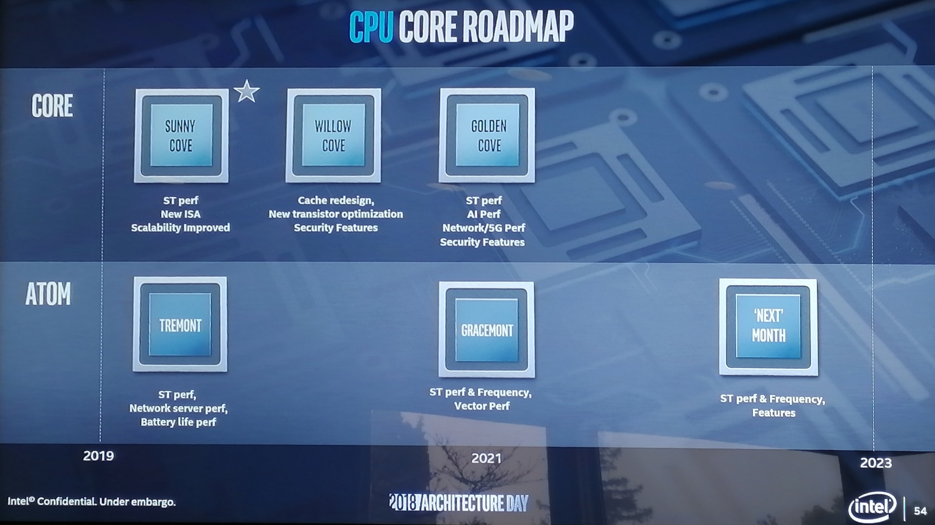
For the high performance Core architecture, Intel lists three new codenames over the next three years. To be very clear here, these are the codenames for the individual core microarchitecture, not the chip, which is an important departure from how Intel has previously done things.
Sunny Cove, built on 10nm, will come to market in 2019 and offer increased single-threaded performance, new instructions, and ‘improved scalability’. Intel went into more detail about the Sunny Cove microarchitecture, which is in the next part of this article. To avoid doubt, Sunny Cove will have AVX-512. We believe that these cores, when paired with Gen11 graphics, will be called Ice Lake.
Willow Cove looks like it will be a 2020 core design, most likely also on 10nm. Intel lists the highlights here as a cache redesign (which might mean L1/L2 adjustments), new transistor optimizations (manufacturing based), and additional security features, likely referring to further enhancements from new classes of side-channel attacks.
Golden Cove rounds out the trio, and is firmly in that 2021 segment in the graph. Process node here is a question mark, but we’re likely to see it on 10nm and or 7nm. Golden Cove is where Intel adds another slice of the serious pie onto its plate, with an increase in single threaded performance, a focus on AI performance, and potential networking and AI additions to the core design. Security features also look like they get a boost.
| Intel Core Microarchitecture Roadmap | |||
| Core Name | Year | Process Node | Improvements |
| Skylake | 2015 | 14 nm | Single Threaded Performance Lower Power Other Optimizations |
| Kaby Lake | 2016 | 14 nm+ | Frequency |
| Coffee Lake | 2017 | 14 nm++ | Frequency |
| Coffee Refresh | 2018 | 14 nm++ | Frequency |
| Sunny Cove | 2019 | 10 nm | Single Threaded Performance New Instructions Improved Scalability |
| Willow Cove | 2020 ? | 10 nm ? | Cache Redesign New Transistor Optimization Security Features |
| Golden Cove | 2021 ? | 7 / 10 nm ? | Single Threaded Performance AI Performance Networking / 5G Performance Security Features |
The lower-powered Atom microarchitecture roadmap is on a slower cadence than the Core microarchitecture, which is not surprising given its history. Seeing as how Atom has to fit into a range of devices, we’re expecting there to be a wide range in capabilities, especially from the SoC side.
The upcoming microarchitecture for 2019 is called Tremont, which focuses on single threaded performance increases, battery life increases, and network server performance. Based on some of the designs later in this article, we think that this will be a 10nm design.
Following Tremont will be Gracemont, which Intel lists as a 2021 product. As Atom is designed to continually push both the performance at the high-end of its capabilities and the efficiency at the low-end, Intel lists that Gracemont will have additional single threaded performance and a focus on increased frequency. This will be combined with additional vector performance, which likely means that Atom will get some wider vector units or support new vector instructions.
Beyond this will be a future ‘mont’ core (and not month as listed in the image). Here Intel is spitballing what this new 2023 core might have, for which the general listing of performance, frequency and features is there.
| Intel Atom Microarchitecture Roadmap | |||
| Year | Process | Improvements | |
| Goldmont | 2016 | 14 nm | Higher Performance Cryptography Features |
| Goldmont Plus | 2017 | 14 nm | Branch Prediction More Execution Larger Load/Store Buffers More Cache |
| - | 2018 | - | - |
| Tremont | 2019 | 10 nm ? | Single Threaded Performance Network Server Performance Battery Life |
| - | 2020 | - | - |
| Gracemont | 2021 | 10 nm ? | Single Threaded Performance Frequency Vector Performance |
| - | 2022 | - | - |
| 'Next Mont' | 2023 | ? | Single Threaded Performance Frequency 'Features' |
As stated above, these are just the microarchitecture names. The actual chips these cores are in will likely have different names, which means a Lake name for the Core microarchitecture. At the event, Intel stated that Ice Lake would have Sunny Cove cores in it, for example.
Another aspect to Intel’s presentations was that future microarchitectures are likely to be uncoupled from any process technologies. In order to build some resiliency into the company’s product line moving forward, both Raja Koduri and Dr. Murthy Renduchintala explained that future microarchitectures will not be process dependent, and the latest products will come to market on the best process technologies available at the time. As a result we’re likely to see some of the Core designs straddle different manufacturing technologies.
Intel also went into a bit of detail on microarchitecture of Sunny Cove.


148 Comments
View All Comments
porcupineLTD - Thursday, December 13, 2018 - link
Can you articulate what you want to say with those links? or how they might contradict me/answer my question?ajc9988 - Thursday, December 13, 2018 - link
What I am saying with those links is that AMD has already evaluated the use of active interposers and is the company that is articulating a data protocol for active interposer routing so that it doesn't matter what each chiplet does on its own data routing, so that any chiplet could be attached to an active interposer and work. Further, in the 2017 white paper, it directly shows the reason that AMD hasn't yet adopted the active interposer is due to costs. Passive interposers can be used, but don't offer the benefit of active interposers. But, the cost of an active interposer is the same as doing a monolithic chip once the active interposer is produced on the 32nm or smaller active interposer. As such, adoption did not yet make sense until the costs are reduced.https://spectrum.ieee.org/tech-talk/semiconductors...
The earlier ones show AMD did research into the optimal topology for active interposers in 2014 and 2015. It shows the optimal core count for the benefit, latencies, etc.
Now, if you look at packaging solutions, say from GF, you find that 2.5D and 3D integration is only available on 32nm and 28nm processes, with 14nm coming soon. https://www.globalfoundries.com/sites/default/file...
I bring up GF doing the packaging as, due to the WSA, even if they cost more than competitors, being able to potentially count the wafers used for the active interposers against the WSA would reduce the fines payed under that contract for doing fabrication at TSMC, making it potentially, on net, cheaper.
Now, there is an article today from Anand saying Intel is releasing the B365 chipset on 22nm. ( https://www.anandtech.com/show/13714/intel-adds-b3... ) Intel was forced to move chipsets back to 22nm due to the 10nm process not being ready for mass deployment which caused a shortage of 14nm capacity. This means Intel could not shut down their 22nm fabs to cut that capacity. As such, a fab needs to stay as close to capacity as possible or else it bleeds money (hence why AMD eventually went fabless). So, Intel using 22nm fabs to do the 22nm active interposer is just Intel making lemonade on tech that few others adopted in the industry yet due to the basis of costs. If you go back to the cost study AMD did, the active interposer at 20nm is around the cost of doing a monolithic die, which is what Intel has done to date. So it isn't really costing them more to add in the active interposer at all, while saving expenditures by keeping the 22nm fabs full of jobs, while having awesome yields on the active interposers due to it being a very mature node with low defect rates, etc. If you examine the amount of area AMD estimated is needed for the logic routers, you can see only 1%-10% area on the active interposer is needed to achieve the goal, meaning the chances a critical defect hits the active interposer is very low.
But, as to it making AMD do it, that is the wrong thinking. AMD already plans to adopt it, just not until the costs of doing so are lower. They will check the IC Knowledge lists to see when costs make sense.
But, if you look at all that data I provided, AMD has all the solutions to the problems encountered with using an active interposer. All they are waiting for is it to be cost effective. Intel isn't leading anything here, other than doing it because they need to justify and subsidize having to keep certain 22nm fabs open because of their chipsets due to the delays in 10nm. Doesn't take a genius to figure it out, just takes someone paying attention to the tea leaves.
ajc9988 - Thursday, December 13, 2018 - link
Also, I forgot to mention that the 2.5D integration of HBM Phy onto a stitched interposer was accomplished last year. This suggests that HBM could be added to an active interposer when AMD eventually does adopt an active interposer. Meanwhile, with only 1-10% of the active interposer being used according to their papers, it leaves room for in the future having elements of the I/O chip being moved to the active interposer as an additional way that things easily could develop. The question is what benefit it would be to produce what on the 32nm or 28nm nodes over having their I/O disintegrated die on 14nm. But I would bet AMD has an idea of what would be better where and will consider it when eventually adopting, considered the detailed paper on routing topology of active interposers in that group of links.porcupineLTD - Thursday, December 13, 2018 - link
Thank you for the detailed response its very informative however its besides my comment, IF Intel ships its chiplet on interposer design in 2019 they will be first (regardless of the reasons or economics behind it), as for AMD not doing it now it's again besides my comment, I wandered if they will do this for ZEN 3 or 4 not ZEN2, ZEN 3 will launch in 2020 when (as far as I know) the WSA expires so what GF does or doesn't do is not that relevant (I would be curious to know about tsmc's or samsung's packaging/interposer offerings). The result (if they implement it in ZEN3/4) will come down to cost (as you point out), socket compatibility (can it be done on the current server socket?) and planning (ZEN3 design is almost done right now so even if the interposer cost is down AMD can't implement it if they didn't predict this one year ago).porcupineLTD - Thursday, December 13, 2018 - link
Also Anandtech, I am not versed in web design, but is it really that hard to have a comment section that doesn't utterly suck? Is it really that hard to introduce an edit function, or at least a delete one?(an upvote/donvote system would be asking for too much).ajc9988 - Thursday, December 13, 2018 - link
Forgive me, many think that Intel is showing through using it that they are significantly ahead in the field of active interposers and 2.5D and 3D chiplet integration, meaning that it would take years for other chip designers to catch up, which isn't the case. So I do apologize for that assumption in regards to you.What those do show is AMD does have plans to do so in the future, it is just a matter of timing. On the socket part, there is a chance they are introducing a new socket in order to support PCIe 4.0 on the upcoming Zen 2 chips, which comes from analyzing their wording from the Next Horizon event on Nov. 6th. Meanwhile, we know that PCIe 5.0 will be finalized potentially in the first half of next year and AMD did mention DDR5 potentially being available for Epyc 3 chips based on Zen 3, but that mainstream chips will not support DDR5 in 2020 (leaves open that TR HEDT platforms may or may not get DDR5 support at that time). Intel has not provided information on when PCIe 4.0, 5.0, or DDR5 will be supported. As such, though, AMD may have backwards compatibility on the CPUs for socket compatibility, but may require a new socket for the new boards containing the new features, which I think is understandable to many in the server and workstation spheres. It is also the reason I may wait for 2020 to upgrade my 1950X rather than next year (if you are going to buy a new board, and there is a chance that board won't contain the new feature sets that release that year, waiting one more year is fine IF your workloads won't suffer for the wait).
But, I read somewhere Intel hinted at 1GB of RAM being integrated with the active interposer processors, acting as an L4 cache. Although not novel (those articles I gave for AMD whitepapers from 2014 and 2015 specifically dealt with on package integration of memory and latencies involved, suggesting we could see some type of 3d memory solution integrated when AMD does incorporate an active interposer), seeing the latencies involved with Crystalwell, which was the eDRAM on Broadwell, suggests that Intel will get a significant uplift in certain workloads, as well as keeping the chip primed and having to go off chip less often for memory calls, which is fantastic. Intel also kept the power delivery part under wraps, which is something that does excite me, but we were given no information about it (possibly bringing FIVR back, which was rumored for Ice and Tiger lake anyways).
Also, on compatibility, part of the reason I gave the article discussing data protocols for active interposers is that the routing is chiplet agnostic, meaning you can integrate parts that have their own internal routing and not effect it. Then just comes down to appropriate socket wiring, which I mentioned they may need new sockets for these features, while just maintaining drop in compatibility for consumer side.
Here is some information on other packaging types out there in the market. I am including them, but as this is just being researched, I am not attesting veracity or relevance, fully. I will have glanced through them, but you understand.
http://s3.amazonaws.com/sdieee/1817-SanDiegoCPMTDL...
"DIGITIMES reports that the new TSMC plant in Chunan will be dedicated to offering the foundry’s in-house developed advanced packaging technologies: CoWoS (chip-on-wafer-on-substrate) and integrated fan-out (InFO) wafer-level packaging, and its newly-unveiled system-on-integrated-chips (SoIC) and wafer-on-wafer (WoW) packaging services."
https://criticalmaterials.org/tsmc-to-set-up-new-f...
https://fudzilla.com/news/pc-hardware/47265-tsmc-t...
https://electroiq.com/2018/10/synopsys-design-plat...
Older article for foundational work from 2014:
https://semiengineering.com/time-to-revisit-2-5d-a...
2016 follow up: https://semiengineering.com/2-5d-becomes-real/
Packaging Market from February 2018:
http://worldherald24.com/2018/02/19/global-3d-ic-a...
Paper and slide show discussing the implementation and challenges of 3D packaging from 2016:
https://smtnet.com/library/files/upload/25d-3d-sem...
Sorry for the data dump at the end. I do apologize about that.
tommybobberson - Saturday, December 15, 2018 - link
just clarifying, do you mean to use such methods, amd would need to rive up production costs which reduces their profit/value. but since intel already has a high production cost, such methods would not affect them?ajc9988 - Wednesday, December 19, 2018 - link
tommybobberson - in a manner of speaking, yes. How much it costs to produce effects margins and pricing. One reason AMD could price the high core chips in such a manner, aside from effective yields for products, is the decreased costs to produce high core count products. If AMD added the active interposer now, it would rise production costs to be the same as a monolithic die, which would then require either an increase in market price of the products or a decrease in margins for their products.Intel, on the other hand, never captured the extra margin of going to chiplets before introducing the stacked chips. That means that the active interposer cost to them is less as the price to do so matches the cost of a monolithic die. As such, Intel can maintain their current pricing while introducing the stacked die on active interposer. Further, due to filling up 22nm fab time (because of 10nm causing a shortage of 14nm fab time which required Intel to move certain lines back to 22nm, likely forcing some plants planned to be closed or retrofitted to remain on 22nm), Intel will be able to help on the cost of 10nm delay, thereby mitigating some of the effects found in not having 10nm up and running by now.
Supercell99 - Friday, December 14, 2018 - link
With all the hackers, PC gaming is dying.sgeocla - Wednesday, December 12, 2018 - link
Fist they mock your chiplets by saying you glue your dies together, then they fail to compete with you and then years after they copy your chiplets and call it revolutionary.This is why Intel can no longer have public presentations of their own failures and have to have privately controlled presentations.