16GB NVIDIA Tesla V100 Gets Reprieve; Remains in Production
by Ryan Smith on May 24, 2018 8:00 PM EST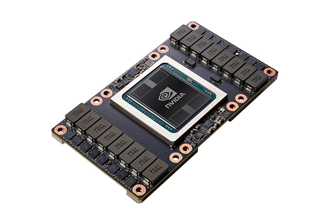
Back in March at their annual GPU Technology Conference, NVIDIA announced the long-anticipated 32GB version of their flagship Tesla V100 accelerator. By using newer 8-Hi HBM2 memory stacks, NVIDIA was able to double the accelerator’s previous 16GB of VRAM to a class-leading 32GB. Meanwhile, at the time company representatives told us that the launch of the 32GB model would be a wholesale replacement of the 16GB model, with the smaller version to be phased out and all future cards to go out as the 32GB model.
However, this week NVIDIA has reached out to inform us that this will not the case, and that the 16GB model is being continued after all.
In a somewhat odd exchange, the official line from the company is that the previous statement – made in the heat of a pre-briefing Q&A session – was in error, and that the 16GB model was never being discontinued. Instead, NVIDIA’s plan has always been to sell the two models side-by-side. Unfortunately, the company hasn’t been able to make it clear why that information wasn’t presented at the show instead; though what I do know is that this wasn’t caught until customers recently started asking questions.
| NVIDIA Tesla/Titan Family Specification Comparison | ||||||
| Tesla V100 (SXM2) |
Tesla V100 (PCIe) |
Titan V (PCIe) |
Tesla P100 (SXM2) |
|||
| CUDA Cores | 5120 | 5120 | 5120 | 3584 | ||
| Tensor Cores | 640 | 640 | 640 | N/A | ||
| Core Clock | ? | ? | 1200MHz | 1328MHz | ||
| Boost Clock | 1455MHz | 1370MHz | 1455MHz | 1480MHz | ||
| Memory Clock | 1.75Gbps HBM2 | 1.75Gbps HBM2 | 1.7Gbps HBM2 | 1.4Gbps HBM2 | ||
| Memory Bus Width | 4096-bit | 4096-bit | 3072-bit | 4096-bit | ||
| Memory Bandwidth | 900GB/sec | 900GB/sec | 653GB/sec | 720GB/sec | ||
| VRAM | 16GB 32GB |
16GB 32GB |
12GB | 16GB | ||
| L2 Cache | 6MB | 6MB | 4.5MB | 4MB | ||
| Half Precision | 30 TFLOPS | 28 TFLOPS | 27.6 TFLOPS | 21.2 TFLOPS | ||
| Single Precision | 15 TFLOPS | 14 TFLOPS | 13.8 TFLOPS | 10.6 TFLOPS | ||
| Double Precision | 7.5 TFLOPS | 7 TFLOPS | 6.9 TFLOPS | 5.3 TFLOPS | ||
| Tensor Performance (Deep Learning) |
120 TFLOPS | 112 TFLOPS | 110 TFLOPS | N/A | ||
| GPU | GV100 | GV100 | GV100 | GP100 | ||
| Transistor Count | 21B | 21B | 21.1B | 15.3B | ||
| TDP | 300W | 250W | 250W | 300W | ||
| Form Factor | Mezzanine (SXM2) | PCIe | PCIe | Mezzanine (SXM2) | ||
| Cooling | Passive | Passive | Active | Passive | ||
| Manufacturing Process | TSMC 12nm FFN | TSMC 12nm FFN | TSMC 12nm FFN | TSMC 16nm FinFET | ||
| Architecture | Volta | Volta | Volta | Pascal | ||
But whatever the internal rationale and timetable on NVIDIA’s part, the end result is that at least for the foreseeable future, NVIDIA is going to be offering multiple V100 capacities across its lineup, including both the SXM2 and PCIe form factors. For NVIDIA's customers then, they now have a choice to make on capacity. The larger version is clocked identically to its 16GB counterpart, so it doesn't have an immediate performance advantage outside of memory capacity. However in cases where a dataset that doesn't fit in the 16GB model fits in the 32GB model, the performance differences can be very significant due to the large impact of memory thrashing; NVIDIA is advertising a 50% performance boost in some memory-limited HPC applications thanks to the larger RAM pool.
Finally, the company also confirmed that these cards will be priced differently. However they aren’t sharing the list prices for the parts, so it’s not clear whether the new pricing structure gives the 16GB model a price cut, or if the 32GB model is being offered at a price premium.
Source: NVIDIA


21 Comments
View All Comments
MrSpadge - Friday, May 25, 2018 - link
He was talking about a price increase, not performance.goldstone77 - Friday, May 25, 2018 - link
Theoretically, it will offer massive performance while greatly reducing in power consumption.edzieba - Friday, May 25, 2018 - link
I'm curious if future production of the V100 16GB will be with 4GB HMB2 stacks, or using binned V100 32GB assemblies with two of the 8GB HBM2 stacks disabled. The former would essentially require two separate SKUs to be maintained (or even two different lines, if the process between the two HBM2 gens is sufficiently different) while the latter would result in a hit to memory bandwidth.MrSpadge - Friday, May 25, 2018 - link
No, they can't just disable half of the memory bandwidth for a product announced otherwise. And mounting the 4Hi or 8Hi stacks is not so different to require different lines. It's just "more of the same" and was designed in the same way. Maybe the 8Hi stacks are a bit higher and require a minor tool adjustment, or that was included from the beginning on (it was always on the roadmap).edzieba - Friday, May 25, 2018 - link
There's never such a thing as a 'minor tool adjustment' in semiconductor manufacture.Spunjji - Friday, May 25, 2018 - link
This doesn't concern semiconductor manufacture, though, it concerns board assembly.CiccioB - Friday, May 25, 2018 - link
As HBM chips can be mounted AFTER being tested, I wonder why they should mount broken memory and then sell a crippled version of the board when they can simply mount perfectly working silicon.edzieba - Saturday, May 26, 2018 - link
That's the problem: you there is still a very high failure rate in the process of assembling 4x dies onto an interposer. And once they're soldered to each other, you can't remove a failed bond and retry, you just have an assembly you either ned to bin without that die active or scrap altogether.CiccioB - Saturday, May 26, 2018 - link
Where did you get the info that there is a high failure rate and that a complete reflow is not possible?ImSpartacus - Friday, May 25, 2018 - link
Doesn't the 32GB V100 use SXM3, which provides 350W of power rather than SXM2's 300W? Not sure of other improvements it might have.