SK Hynix Adds HBM2 to Catalog: 4 GB Stacks Set to Be Available in Q3
by Anton Shilov on August 1, 2016 10:00 AM EST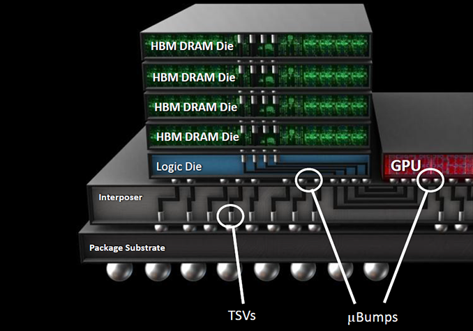
SK Hynix has quietly added its HBM Gen 2 memory stacks to its public product catalog earlier this month, which means that the start of mass production should be imminent. The company will first offer two types of new memory modules with the same capacity, but different transfer-rates, targeting graphics cards, HPC accelerators and other applications. Over time, the HBM2 family will get broader.
SK Hynix intends to initially offer its clients 4 GB HBM2 4Hi stack KGSDs (known good stack dies) based on 8 Gb DRAM devices. The memory devices will feature a 1024-bit bus as well as 1.6 GT/s (H5VR32ESM4H-12C) and 2.0 GT/s (H5VR32ESM4H-20C) data-rates, thus offering 204 GB/s and 256 GB/s peak bandwidth per stack. Earlier this year a representative for SK Hynix revealed plans (in an interview with Golem.de) to start volume production of 4 GB HBM2 KGSDs in Q3 and the addition of the devices into product catalog confirms this information. Keep in mind that memory companies usually make announcements about the start of mass production when they are ready to deliver the first batch of new DRAM to a customer(s). Therefore, it is possible that SK Hynix may already be producing HBM2 stacks.
| Specifications of SK Hynix's HBM2 Memory Chips | ||||||||
| Part Number | Density | Data Rate | Bandwidth per Stack |
Packaging | Feature | Availability | ||
| H5VR32ESM4H-20C | 4 GB | 2.0 GT/s | 256 GB/s | 5mKGSD | 4Hi stack, VDD/VDDQ=1.2V | Q3'16 | ||
| H5VR32ESM4H-12C | 1.6 GT/s | 204 GB/s | ||||||
As outlined in our article published earlier this year, HBM2 memory can stack two, four or eight DRAM devices (2Hi, 4Hi, 8Hi stacks) interconnected using through silicon vias (TSVs) on a base logic die per KGSD (known good stacked die). Each DRAM device features two 128-bit channels, which use DDR signaling with a 2n prefetch architecture (256 bits per memory read and write access) and can operate at their own frequency or even in their own mode. SK Hynix uses 21 nm process technology to make its HBM2 memory and eventually plans to offer 2 GB and 8 GB KGSDs (featuring two or eight 8 Gb DRAM ICs) in addition to 4 GB stacks, aimed at providing memory for various applications. All HBM2 memory products from the company will have 1.2 V VDD/VDDQ and will come in new packages featuring 7.75 mm × 11.87 mm (91.99 mm2) dimensions.
Samsung Electronics began to mass produce its 4 GB 4Hi stack HBM2 KGSDs featuring 2 GT/s data-rate earlier this year and NVIDIA employed the new chips for its GP100 GPU. The first NVIDIA-branded card to use the HBM2 is the Tesla P100 compute accelerator, which has 16 GB of HBM2 memory with 720 GB/s bandwidth (as the DRAM interface operates at about 1.4 GT/s data-rate).

Speaking of HBM2 usage by commercial SoCs, last year SK Hynix said that it worked with 10 companies on various projects (including ASICs, x86 processors, ASSPs and FPGAs) featuring HBM memory (both generations), which indicates that the interest for multi-layer high-bandwidth DRAM is here. However, so far only AMD and NVIDIA have introduced actual products featuring HBM and HBM2.
When it comes to the original HBM, it is worth to mention that SK Hynix has removed such stacks from its catalog. It is unknown whether the company continues to ship them to interested parties, but given the fact that there are not a lot of products that utilize HBM1 today, small scale shipments should not be a problem (at least, until SK Hynix phases out its 29 nm production lines). Meanwhile, since HBM2 is here, it is feasible to assume that we are not going to see many new devices utilizing HBM1.
Source: SK Hynix


43 Comments
View All Comments
wumpus - Tuesday, August 9, 2016 - link
I'd be even more partial to an "APUless" Zen with HBM for general CPU work. The APU only makes sense if they can get *anybody* on the heterogenous programming train, and that still isn't happening (while physX does fine), or you are using a stripped down device (presumably mobile and ChromOS level low).Mostly the idea is that if you have plenty of cores (especially for a Zen server, but that's dreaming) you will have more pressure than the [on die] caches can handle, and thus more bandwidth than an ordinary DDR4 bus can handle. Hopefully HBM2 to the rescue.
While I'm really dreaming, instead of HBM misses going to DDR4, use 3dXpoint for main memory (like Intel won't block Micron from selling it for that. But given time...). 64GB of "main storage" that is part virtual ram and part disk cache would really upset the memory hierarchy.
- further notes:
Unless things have changed, calling HBM2 "on die" is really deceptive. It *is* on die, on but an adapter die that both the HBM ram and GPU[/APU/CPU] dice are bonded to.
The fact that the stuff is called "high bandwidth memory" and not "low latency memory" doesn't mean it makes a bad cache. It might need a long lines or otherwise multiple access at once, but that is to be expected on a multi-core CPU. And while a L1/L2/L3 might be all about low latency, the point of your L4 is about reducing bandwith to "main memory" (DRAM/3dXpoint/SLC?).
LarsBars - Monday, August 1, 2016 - link
Could AMD theoretically make 8GB versions of Fiji using HBM2 in 2016? Similar to the way that GP104's memory controller can do GDDR5 and GDDR5X, could we feasibly see an RX 490 with Fiji and 8GB HBM2? I think one of the Fury lineup's biggest drawbacks was memory capacity. Just curious.DanNeely - Monday, August 1, 2016 - link
In theory yes; but doing so would require major amounts of design work and revalidation in manufacturing. Unless they started it a number of months ago, by the time they finish they'll be right on top of the planned Vega launch dates. The ideal time to have done this would've been when Fiji was first being designed a few years ago.LarsBars - Monday, August 1, 2016 - link
Ahh gotcha. Thanks for the explanation. Bring on Vega!Eden-K121D - Tuesday, August 2, 2016 - link
HBM 1 standard was updated to support 2GB stacks so yes a 4*2 GB configuration is possiblehaukionkannel - Tuesday, August 2, 2016 - link
Also hbm2 is more expensive than hbm1 and Fuji is not very badly memory starved. So better increase power by vega and add more memory for future games. But it should be possible. Not sure though that it would be difficult. If there is as Many memory stacks as in normal fury, increasing the high of memory stack could be as easy as drop in replasement.ChefJeff789 - Monday, August 1, 2016 - link
I wold love to see AMD create a Zen APU with a couple of stacks of HBM2. As to the market this would target, I'm not totally certain, but I've long wanted to see Intel or AMD create a compelling product that integrates everything into a single package much like a console does already. If the accompanying GPU is good, something like this would replace every set-top box I own along with my desktop/Plex serverutroz - Monday, August 1, 2016 - link
I can say 100% AMD is going to have Zen APU's with HBM2 and has had this planned for a long time.Laststop311 - Monday, August 1, 2016 - link
Zen APU's with gpu's large enough for 1080p 60 fps high settings will take a huge bite out of the discrete gpu market. Which AMD is already losing so they really have nothing to lose having the apu cannibalizing the discrete market. Nvidia has far more to lose from that.tarqsharq - Tuesday, August 2, 2016 - link
2gb HBM not even HBM2 would be amazing for an APU.